1. DESCRIPTION
The TMP512 (dual-channel )and TMP513triple-channel)are system monitors that includeremote sensors, a local temperature sensor, and aigh-side current shunt monitor. These systemmonitors have the capability of measuring remotetemperatures, on-chip temperatures, and systemoltage/power/current consumptionThe remote temperature sensor diode-connectedtransistors are typically low-cost, NPN- or Pnp-type transistors or diodes. no calibration needed.
TMP512/513作为系统检测器使用。可以监控远程温度、本地温度和电压电流。
远程温度传感器连接的晶体管通常是低成本的NPN或PNP晶体管。并且无需校准。
2. Typical Application Circuit
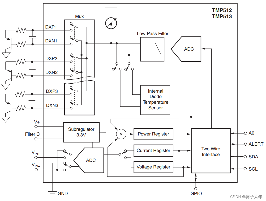
上图是一个典型应用电路图。
1)DXP1/DXN1 - 3 远程温度传感器
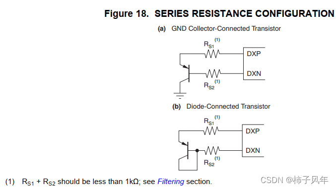
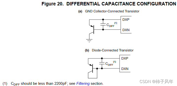
DXP1/DXN1 - 3是远程温度传感器的 3组对外接口,分别接到三极管的两端。
同时接了一对串行电阻(见图18)和一个差分电容(见图20)。下图中展示了参考连接方式和阻容值要求,按照他的来 | 具体为啥这样做暂不关心……
2)温度测量
三路远程温度传感器和一路本地温度传感器,经过“Low pass filter”低通滤波器,输入到ADC测量电路,芯片再根据控制寄存器参数将结果传输到只读温度寄存器
3)总线电压
V+和Filter C作为BUS测量电路的输入送到ADC,用于测量总线电压,输入电压范围是0~26V。
如下引用和下图,展示了手册提供的三种不同连接配置。
Configuration 1 has V + and VIN + tied together . V +supplies the subregulator , which in turn supplies the3 . 3V to the Filter C pin and the internal die . With theV + supply range of 4 . 5V to 26V connected to theshunt voltage , the bus voltage range cannot go tozero and is limited to 4 . 5V to 26V.
Confiquration 2 has V + to the subrequlator withoutany other connections . Under this confiquration . thebus voltage range can go from 0V to 26V , because itis not limited to 4.5 as in Configuration 1.
Configuration 3 has the subregulator V + and Filter Cpins shorted together . V + is limited to 3V to 5 . 5Vbecause the Filter C pin supplies the internal die ; itcannot exceed this voltage range . The bus voltagerange can go from 0V to 26V , because it is not limitedto 4 . 5V as in Confiquration.

4)Shunt分流器测量
分流电阻为建议最大不超过0.5欧姆的电阻。
ADC测量电阻两端的电压和电流,进而得到分流器电压值、电流值以及功率值。
3. Register Table
00/01为通用的配置寄存器,02为状态配置寄存器。
实际使用过程中,如果不需要芯片输出报警状态,则用默认值即可。具体要查看00和01的每个16bit寄存器值的每一个bit定义。
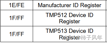
1E和1F为ID寄存器,可用于验证芯片是否正常工作。
08为本地温度传感器结果。理论上,只要芯片正常工作,其寄存器值的转换结果就应该是与真实环境温度相符合。
09/0A/0B为远程温度传感器结果。只要芯片正常+外部接法正确,结果值就应该是正常的,否则就要查看外部接法和芯片工作状态。
04/05为分流器和总线电压,也是只需要芯片正常+外部接法正确。
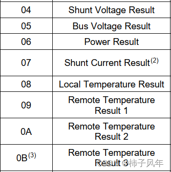
05/06则为电流测量值和功率值,该值不仅需要芯片正常+外部接法正确,还要进行软件配置。否则读到的都是0。
即配置Shunt Calibration Register 15寄存器 ,该寄存器是“根据最大电流值计算得到的测量最大值”。具体转换规则参考手册 “ Calibration Register and Scaling ”部分。

如下提供一段简单的校准寄存器设置代码:
const int vshunt_max = 8*40;//分流器最大电压:毫伏
const int shunt_uohms = 20000;//分流器电阻:微欧姆
Tmp513.curr_lsb_ua = (vshunt_max*1000*1000/shunt_uohms) *1000/32767;//PGA=8 "/1000"<=>uohms=1000
Tmp513.pwr_lsb_uw = Tmp513.curr_lsb_ua *20;
Temp = Tmp513.curr_lsb_ua/1000;
Temp = (Temp==0)?40960:40960/Temp;if( Tmp513_Write(TMP513_SHUNT_CAL, Temp) != 0)
goto TMP513_ERROR_INIT;
4. 其它
1、本篇文章参考了 TMP513 的芯片手册,立创商城上就能搜到。
2、参考 github上 linux源码的驱动文件中的tmp51x.c
[v8,2/2] hwmon: Add driver for Texas Instruments TMP512/513 sensor chips. - Patchwork (kernel.org)
3、I2C驱动
与正常的I2C驱动完全一样。
遇到的I2C驱动简单分为3类:
1)没有寄存器地址,只需要写数据
如一般的IO扩展芯片,先写地址,再写入8bit数据,分别控制8个IO输出的高低电平。
2)有寄存器地址,数据为8bit
先写8bit地址,收到ack后,再写入8bit 寄存器地址 等待ACK,然后再写入8bit数据。
3)有寄存器地址,数据为16bit
TMP513就是16bit。
先写8bit地址,收到ack后,再写入8bit 寄存器地址 等待ACK,然后再写入8bit高字节,再再写入8bit低字节。
//参考程序
static uint8_t mI2C_Read_2byte(uint8_t reg, uint16_t *pData)
{
uint8_t byte[2];
if(HAL_I2C_Mem_Read(&hi2c3, TMP513_DEV_ADDR, reg, I2C_MEMADD_SIZE_8BIT, byte, 2, 1000) == 0)
{
*pData = byte[0]*256+byte[1];
return TMP513_OK;
}
else
return TMP513_ERROR;
}
static uint8_t mI2C_Write_2byte(uint8_t reg, uint16_t data)
{
uint8_t byte[2];
byte[0] = data>>8;
byte[1] = data&0x00FF;
return HAL_I2C_Mem_Write(&hi2c3, TMP513_DEV_ADDR, reg, I2C_MEMADD_SIZE_8BIT, byte, 2, 1000);
}