1、Nand Flash 读取步骤
- 从主存中读到Cache
- 从Cache读取数据
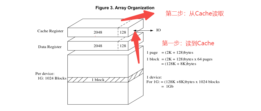
2、从主存读到Cache
2.1 在标准spi接口下读取过程
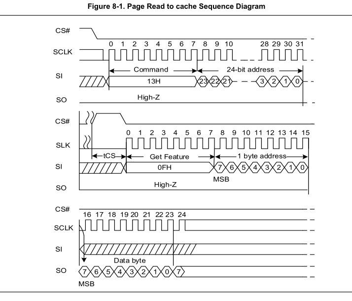
发送Page Read to Cache command(13H)
发送page地址 24位
检查寄存器位OIP,读取flash状态,等待主存读cache操作完成
读取hwecc位,判断是否超过ecc纠错的最大限度
rt_err_t spinand_read_dataload(struct rt_spi_device *spi,  uint8_t u8Addr2, uint8_t u8Addr1, uint8_t u8Addr0)
{


    rt_err_t result = RT_EOK;
    uint8_t au8Cmd[4] = {

    CMD_PAGE_READ_TO_CACHE, u8Addr2, u8Addr1, u8Addr0};
    uint8_t u8SR;


    if ((result = rt_spi_send(spi, &au8Cmd[0], sizeof(au8Cmd))) == 0)
        goto exit_spinand_read_dataload;

    if (spinand_isbusy(spi))
    {


        result = -RT_EIO;
        goto exit_spinand_read_dataload;
    }

    u8SR = spinand_hwecc_status_get(spi);
    if ((u8SR != 0x00) && (u8SR != 0x01))
    {


        result = -RT_MTD_EECC;
        LOG_E("Error ECC status error[0x%x].", u8SR);
    }

exit_spinand_read_dataload:

    return result > 0 ? RT_EOK : -RT_ERROR;
}
2.2 测试时序(SPI频率30MHz)
- 发送读取指令和地址:
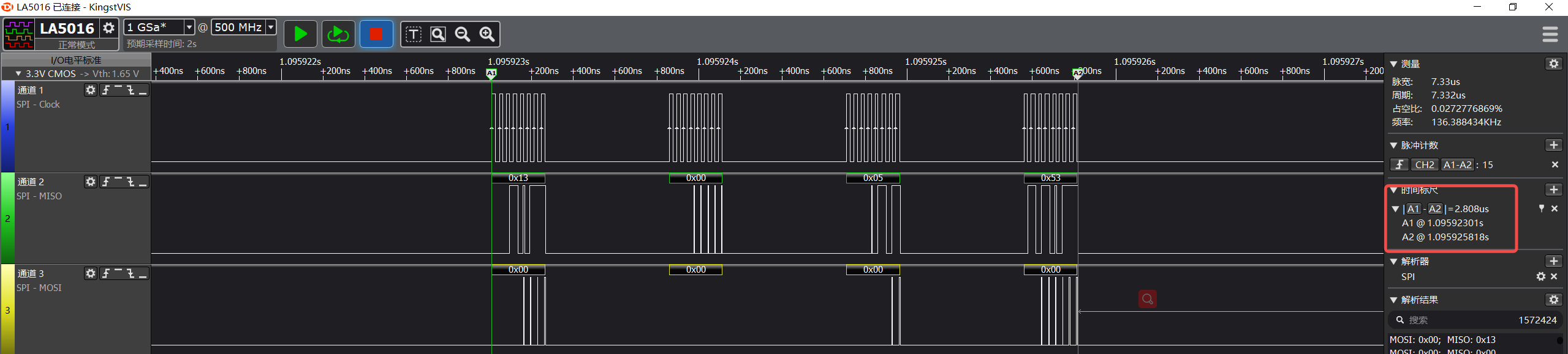
- 检查寄存器位
OIP,读取flash状态,等待主存读cache操作完成
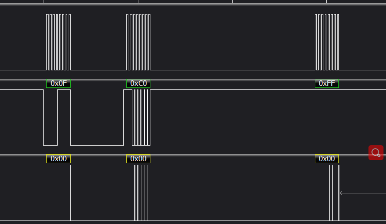
OIP位至0,主存读cache操作完成
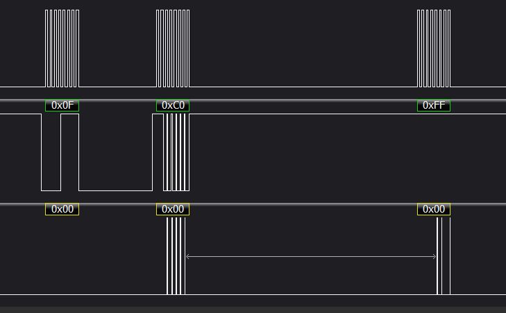
- 整个过程消耗时间
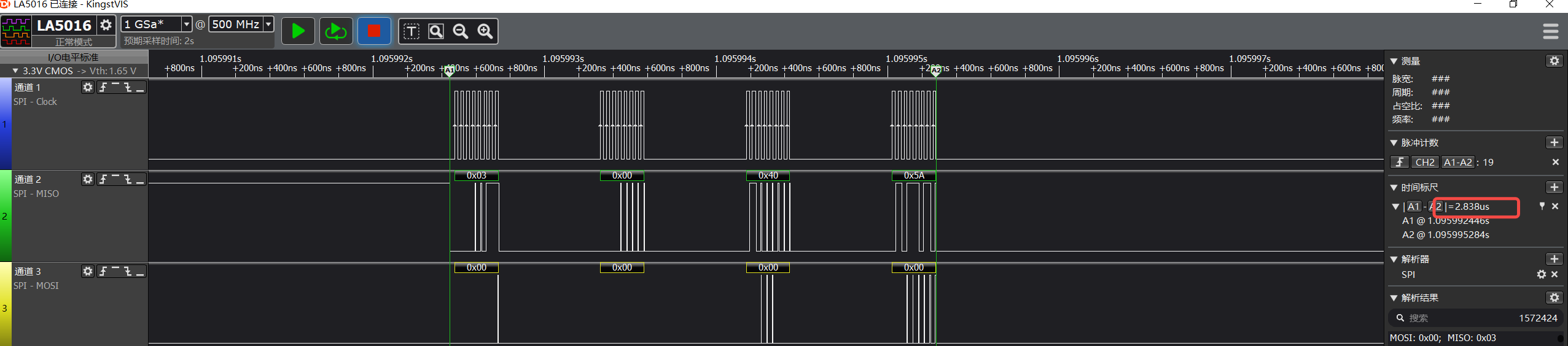
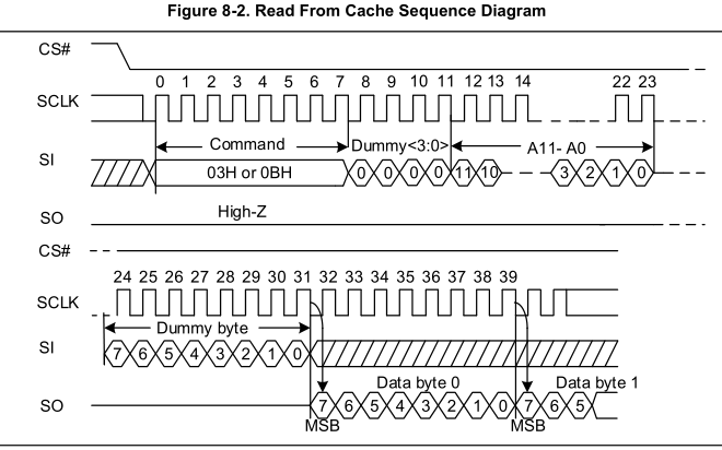
3.从Cache读取数据
3.1在标准spi接口读取过程
发送Read From Cache command(03H)
发送page地址 24位
发送数据
	rt_err_t spinand_normal_read(struct rt_spi_device *spi, uint8_t u8AddrH, uint8_t u8AddrL, uint8_t *pu8Buff, uint32_t u32Count)
	{


	    uint8_t au8Cmd[4] = {

    CMD_READ_FROM_CACHE, u8AddrH, u8AddrL, DUMMY_BYTE};

	    return rt_spi_send_then_recv(spi, &au8Cmd[0], sizeof(au8Cmd), pu8Buff, u32Count);
}
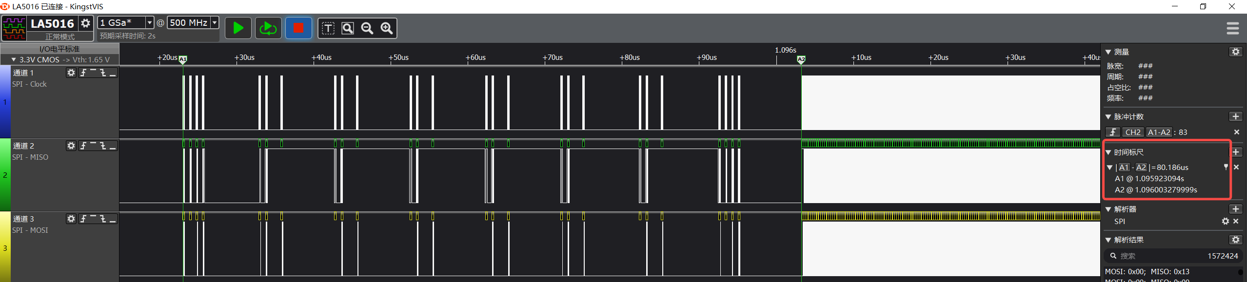
测试时序
发送读取指令和地址: