文章目录
应用场景——什么时候需要刷cache
1、在不同硬件之间共享数据时
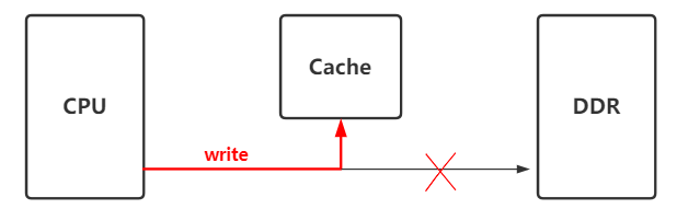
场景:CPU往src地址处写入了一串数据,然后交给Crypto硬件进行加解密处理,加解密后的数据放在了dst地址处,然后cpu读取dst地址处的数据获取结果。
(1)、cpu在往内存(src地址)写数据时,cache中会缓存这些数据,并没有立即同步到DDR, 只有该地址在cache中被换出去时候,才会同步到ddr
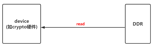
(2)、Device和ddr直接无cache,device直接从ddr(src地址)中读取数据, 此时当然读不到前面cpu写入的数据.
解决办法, 在device读取ddr数据之前, 先做__flush_dcache_area, 将cache数据刷到到内存
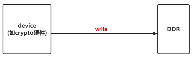
(3)、Device和ddr直接无cache,device将数据直接写入到ddr(dst地址)
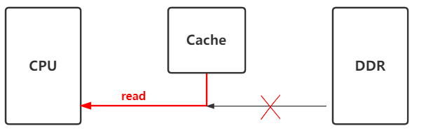
(4)、cpu再次读取该地址(dst)数据时,发现cache中已经缓存了该地址数据,就会直接从cache中拿,就不会去ddr中拿了. 就拿不到device写入到ddr中的数据了.
解决办法:device写入数据到DDR后,调用__invalid_dcache_area, 让cache中缓存的数据无效,这样cpu再次读取的时候,发现cache中的缓存无效,就会从DDR中读取
2、在不同系统之间共享数据时(如linux / optee)
如果是VIVT的cache(virtual index virtual tag),在linux kernel中有一份地址空间,在optee中也有一份地址空间.
linux kernel和optee通过share memory进行通信. 对于同一块物理地址,在linux kernel和optee中映射的虚拟地址是不同的, 所以对于该物理地址的数据,在linux kernel和optee中,缓存到了不同的cache中:
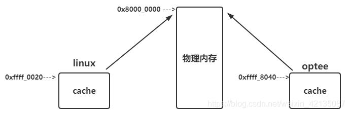
当linux往该区域写入数据时,并没有直接写入到物理内存,而是写到了cache中。只有cache中的数据将被换出去时,cache中的数据才会被真正写入到内存;
而TEE去该区域读取数据,该区域如果在TEE中miss了,那么TEE会到物理内存中读取,此时拿到的不是有效数据。
而如果在TEE中hit,此时会到Cache中读取数据,该cache并不是linux缓存共享物理buf的那段cache,显然也拿不到有效数据。
解决方案: linux中写入数据后,请flush_dcache,在optee读取数据之前,请先invalid_dcache。
cache原理介绍
1、ARM cache的层级关系
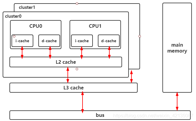
在ARM architecture的设计中,cache有三级: L1、L2、L3.
L1 cache是每个arm core私有的,L1 Cache又分为i-cache、d-cache,
L2 cache是每个cpu cluster中Arm core共享的,不区分icache和dcache.
L3 cache是所有cpu cluster共享的.
以A76核为例:
(1)、L1 d-cache 和 L1 d-cache都是64KB,4路256组相连,每个cache line是64bytes. 这个配置由ARM Core决定的,是SOC中无法修改
(2)、L2 cache是8路相连的cache,大小可选:128KB、256KB、512KB, 这个配置基本也有ARM Core决定,但是在SOC侧由三种size可选
(3)、L3 cache是由SOC侧设计.
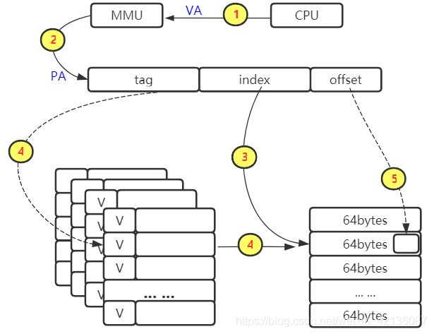
ARMv8的多级cache访问内存的框图:
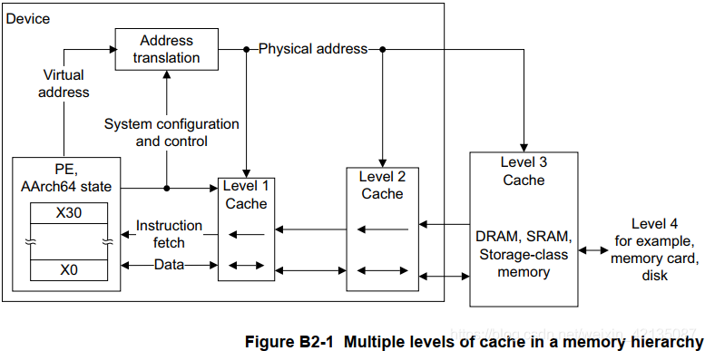
在armv8中,当cpu需要访问一个虚拟地址、首先需要经过MMU转换成物理地址,然后再到L1 L2 L3中查询相应数据
2、Cache的一些基本概念
(1)、cache的种类
PIPT : Physically Indexed, Physically Tagged
VIVT : Virtually Indexed, Virtually Tagged
VIPT : Virtually Indexed, Physically Tagged ---- 在armv8的芯片中,一般都是这种

(2)、cache的连接方式
直接映射缓存(Direct mapped cache)
两路组相连缓存(Two-way set associative cache)
全相连缓存(Full associative cache)
-
直接映射缓存:
优点:硬件设计上会更加简单、成本也较低
缺点: 容易出现cache颠簸(cache thrashing)影响性能 -
两路组相连缓存
优点:减少cache颠簸出现频率
缺点: 增加硬件设计复杂读、成本较高(需要比较多个cache line的TAG) -
全相连缓存
优点:最大程度的降低cache颠簸的频率
缺点: 增加硬件设计复杂读、成本较高(需要比较多个cache line的TAG)
这种cache的地址中,无需index了。
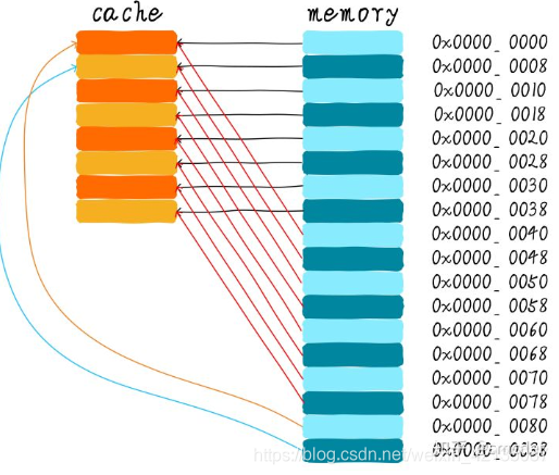
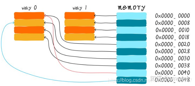
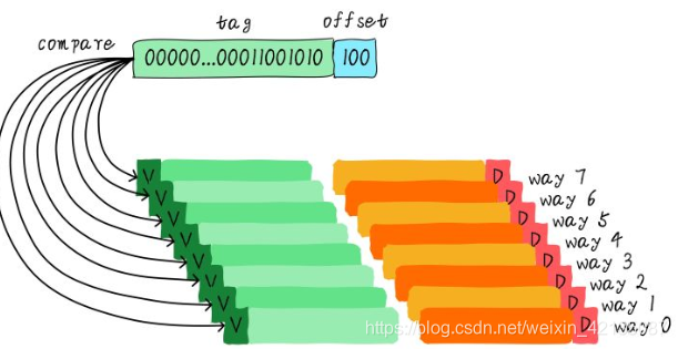
(3)、cache line的查询过程
举例:L1-dcache :一个大小64KB的cache,4路256组相连,cache line为64bytes
在L1-dcache中的查询过程: cpu发起一个虚拟地址,经过MMU转换为物理地址,根据index去查找cache line(因为是四路相连的cache,所以可以查询到4个cache line),然后对比TAG(先看invalid位,再对比TAG值),然后再根据offset找到具体的bytes取出数据
注意,再A76中,L1-dcache是“一个大小64KB的cache,4路256组相连,cache line为64bytes”的cache; L2-cache是 “8路相连的cache,大小为128KB”. 如果L1-dcache查询miss了,则会继续再查询L2-cache
(4)、cache line / entry / set / way的概念

3、A76的Cache
L1 i-cache :64KB,4路256组相连,cache line位64bytes
L1 d-cache :64KB,4路256组相连,cache line位64bytes
L2 cache :8路相连的cache,大小可选-128KB, 256KB, or 512KB
L1 TLB i-cache :全相连(fully associative),48 entries , 支持4KB, 16KB, 64KB, 2MB,32M page-size
L1 TLB d-cache :全相连(fully associative),48 entries ,支持4KB, 16KB, 64KB, 2MB,512MB page-size
L2 TLB cache : 5 ways, 1280 entries
3、armv8的cache寄存器小结
(1)、常用的寄存器
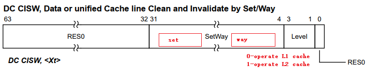
DC CISW, Data or unified Cache line Clean and Invalidate by Set/Way
(Clean Invalidate Set Way)
DC CISW, <Xt>
举个例子:
DC CSW, Data or unified Cache line Clean by Set/Way
DC CSW, <Xt>

DC CVAU, Data or unified Cache line Clean by VA to PoU
DC CVAU, <Xt>

DC ZVA, Data Cache Zero by VA
DC ZVA, <Xt>

IC IALLU, Instruction Cache Invalidate All to PoU
IC IALLU{, <Xt>}
IC IALLUIS, Instruction Cache Invalidate All to PoU, Inner Shareable
IC IALLUIS{, <Xt>}
IC IVAU, Instruction Cache line Invalidate by VA to PoU
IC IVAU{, <Xt>}

DC CIVAC, Data or unified Cache line Clean and Invalidate by VA to PoC
DC CVAC, Data or unified Cache line Clean by VA to PoC
DC CVAP, Data or unified Cache line Clean by VA to PoP
DC GVA, Data Cache set Allocation Tag by VA
DC GZVA, Data Cache set Allocation Tags and Zero by VA
DC IGDSW, Data, Allocation Tag or unified Cache line Invalidate of Data and Allocation Tags by Set/Way
DC IGDVAC, Data, Allocation Tag or unified Cache line Invalidate of Allocation Tags by VA to PoC
DC IGSW, Data, Allocation Tag or unified Cache line Invalidate of Allocation Tags by Set/Way
DC IGVAC, Data, Allocation Tag or unified Cache line Invalidate of Allocation Tags by VA to PoC
DC ISW, Data or unified Cache line Invalidate by Set/Way
DC IVAC, Data or unified Cache line Invalidate by VA to PoC
DC CVADP, Data or unified Cache line Clean by VA to PoDP
(2)、armv8.5 memory-tag相关的cache寄存器
ARMv8.5-MemTag:
DC CGDSW, Data, Allocation Tag or unified Cache line Clean of Data and Allocation Tags by Set/Way
DC CGDVAC, Data, Allocation Tag or unified Cache line Clean of Allocation Tags by VA to PoC
DC CGDVADP, Data, Allocation Tag or unified Cache line Clean of Allocation Tags by VA to PoDP
DC CGDVAP, Data, Allocation Tag or unified Cache line Clean of Data and Allocation Tags by VA to PoP
DC CGSW, Data, Allocation Tag or unified Cache line Clean of Allocation Tags by Set/Way
DC CGVAC, Data, Allocation Tag or unified Cache line Clean of Allocation Tags by VA to PoC
DC CGVADP, Data, Allocation Tag or unified Cache line Clean of Data and Allocation Tags by VA to PoDP
DC CGVAP, Data, Allocation Tag or unified Cache line Clean of Allocation Tags by VA to PoP
DC CIGDSW, Data, Allocation Tag or unified Cache line Clean and Invalidate of Data and Allocation Tags by Set/Way
DC CIGDVAC, Data, Allocation Tag or unified Cache line Clean and Invalidate of Data and Allocation Tags by VA to PoC
DC CIGSW, Data, Allocation Tag or unified Cache line Clean and Invalidate of Allocation Tags by Set/Way
DC CIGVAC, Data, Allocation Tag or unified Cache line Clean and Invalidate of Allocation Tags by VA to PoC
(3)、PoU、PoC、PoP、PoDP 的概念
PoU : Point of Unification 到L2
PoC : Point of Coherency 到L3
PoP : Point of Persistence 到DDR
PoDP : Point of Deep Persistence