基本电路结构
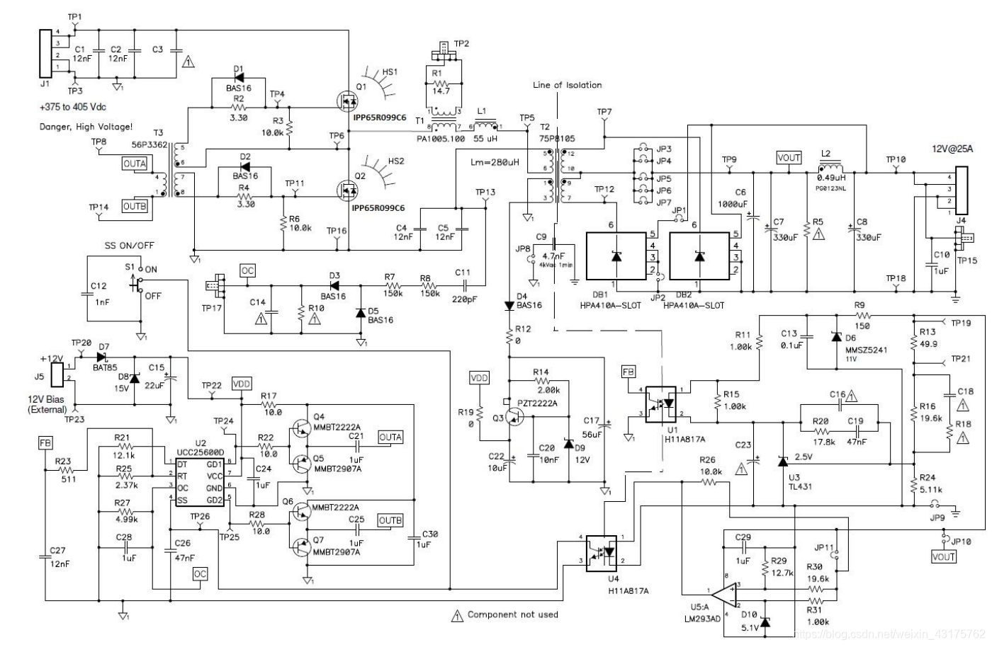
按照此电路进行配置,即可。
值得注意的是,本电路的输出电压为12V,其相关的电路参数设计也都是基于400V->12V的配置进行设计的。若要改变电路的输入输出值,则以下电路参数需要进行相关的改变:
- 输出电压反馈的补偿网络
- 检测谐振电容电压以进行过流保护OC的RC网络
- 变压器的变比
相关的Python代码稍后奉上,代码将运行两次:
- 运行现有的电路配置,得到与上图相同的电路参数值(主要是电阻和电容),验证代码原理的正确性;
- 输入定制的电路配置,得到我们需要的电路参数值。
设计原理:
TL431的反馈回路的设计
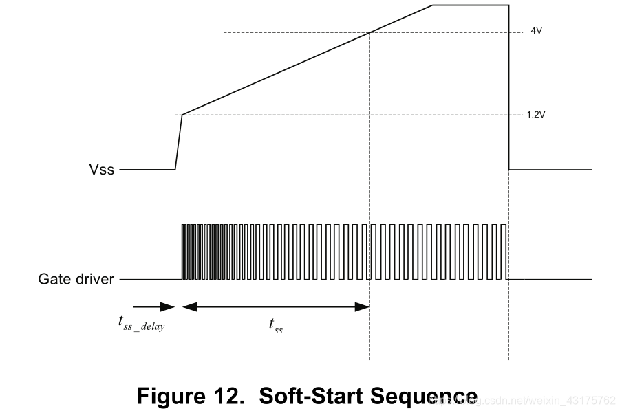
Feature Description
Soft Start
-
软起动时序
-
SS 引脚同时也是芯片的ON/OFF引脚,当Vss低于1V的时候, the device is disabled.
-
当开始启动的时候,如果SS引脚的电压低于1.2V,此时它的输出电流为175uA。因此,上图中的延时
-
当SS引脚的电压高于1.2V时,此时驱动信号的频率由SS pin的电压和RT引脚的电流共同决定。
-
-
当SS引脚的电压达到4V的时候,输出频率由 决定。因此,软起动时间为
-
To ensure reliable operation, the gate drivers restart with GD2 turning high. This prevents uncertainty during system start up.
Overcurrent Protection (OC pin)
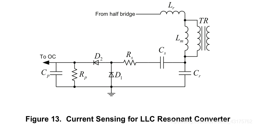
- The general concept of this sensing method is that the ac voltage across the resonant capacitor is proportional to load current. 这种检测过流的原理是基于谐振电压和负载电流是成正比的。
- 电路参数的设计如下表
| Name | Function | Design Equation |
|---|---|---|
| Transfer ac voltage across resonant capacitor into current source | ||
| Blocking dc voltage on resonant capacitor | ||
| Load resistor of the current source | ||
| Filter capacitor |