EDITORIAL words
In the design of the digital logic circuit, a frequency divider circuit is a basic unit. Typically used for a given frequency division, to obtain the desired frequency. Divide in the FPGA design has been served a very important role, but when it comes to frequency, I believe many people have thought of using the counter to get the desired clock frequency, but the problem is using only counter to divide , can only be realized even frequency division, but if need three frequency, frequency-fifth, seventh and so on odd class frequency divider, then how should I do it? here, dream-wing brothers to introduce a way to achieve an arbitrary integer the method of frequency division.
The principle
This method is also the use of the counter to achieve, of course, we are using a state machine to achieve. We first define the number of frequency-divided clock high and a low number, in the first state, when the counter value is smaller than the number of frequency-divided clock low when the output level is low, equal to the number of low level when the output is inverted and clears the counter to jump to the next state. In this state, when the counter time is less than the number of high frequency-divided clocks, the same output level, when the counter value is equal to the number of high level, the output inverted clears the counter to jump to the state , this can be achieved at any frequency.
system framework
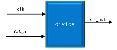
Port Description top module
| Port Name |
Port Description |
| clk |
The system clock 50Mhz |
| rst_n |
Low-level system reset signal |
| clk_out |
Divided clock output |
Code Analysis
| /**************************************************** * Engineer: Dream Brother Wing * QQ : 761664056 * The module function: arbitrary frequency module ***************************************** ************ / 01 module divide( CLK 02 , // system clock input RST_N 03 , // low reset system 04 clk_out // divided clock output 05 ); 06 07 Parameter HW = . 3 ; // output clock high level width 08 Parameter LW = 2 ; // output clock low level width 09 10 INPUT CLK ; // system clock input . 11 INPUT RST_N ; // low-level system reset 12 is Output CLK_OUT ; // divided clock output 13 14 reg clk_out; 15 REG [ 31 is : 0 ] COUNT ; // counter 16 reg state; //状态寄存器 17 18 always @ (posedge clk or negedge rst_n) 19 begin 20 if (!rst_n) //异步复位 21 begin 22 clk_out <= 1'b0; //赋初值 23 count <= 0; 24 state <= 0; 25 end 26 else 27 case (state) 28 0 : if (count < LW-1) //输出低电平个数比较器 29 begin 30 count <= count + 1; 31 state <= 0; 32 end 33 else //输出低电平个数等于设定的低电平个数 34 begin 35 count <= 0; //计数器清零 36 clk_out <= 1'b1; //输出变为1 37 state <= 1; 38 end 39 40 1 : if (count < HW-1) //输出高电平个数比较器 41 begin 42 count <= count + 1; 43 state <= 1; 44 end 45 else //输出高电平个数等于设定的高电平个数 46 begin 47 count <= 0; //计数器清零 48 clk_out <= 1'b0; //输出变为0 49 state <= 0; 50 end 51 default : state <= 0; 52 endcase 53 end 54 55 endmodule |
第7~8行定义了2个参数,一个是输出高电平的个数,一个是低电平的个数,比如HW=3,LW=2输出就是一个5分频的时钟,
比如HW=3,LW=3输出就是一个6分频的时钟,可见只要改变HW和LW的值就可以实现任意分频。第18~53行就是利用状态机来实现分频的过程,用2个状态来计数输出高电平个数和低电平个数。
编写测试代码如下:
| /**************************************************** * Engineer : 梦翼师兄 * QQ : 761664056 * The module function : 任意分频测试模块 *****************************************************/ 01 `timescale 1ns/1ps //仿真时间单位是ns,仿真时间精度是ps 02 module tb; 03 04 reg clk, rst_n; //仿真激励时钟,复位信号 05 06 wire clk_out; //仿真输出分频信号 07 08 initial begin 09 clk = 0; //clk时钟信号初始化 10 rst_n = 0; //rst_n复位信号初始化 11 #200.1 12 rst_n = 1; //200.1ns之后,复位结束 13 end 14 15 always #10 clk = ~clk; //产生50Mhz时钟信号 16 17 divide divide( //把激励信号送进diveder模块 18 .clk(clk), 19 .rst_n(rst_n), 20 .clk_out(clk_out) 21 ); 22 23 endmodule |
仿真分析

我们输入的时钟是50Mhz,一个周期是20ns,输出5分频的时钟,周期是100ns,可见我们的设计是正确的。
我们修改分频模块的参数将HW改为3,LW改为3,仿真波形如下:

同样输入的时钟是50Mhz,一个周期是20ns,输出6分频的时钟,周期是120ns,可见我们的设计是正确的。