2.3 sensor technology

FIG pixel structure and evolution of 2.11; (A) the basic structure of the pixel: accumulation units and the photodiode; (B) Active pixel, increasing the field amplification; (c) 4-T pixel configuration Active: accumulation and read-out module separating
Digital camera imaging sensor function like the old camera film. Light passing through the lens system is transformed into an electrical signal. The electrical signals are suitably processed in a standard format in the pipeline end of the memory. FIG. 2.11 (a) shows the basic structure of a pixel: a photodiode (light into electrical signals), an accumulation unit (capacitor) and a switch. This structure is also known as Passive pixel. The advantage of this construction is to maximize the fill factor.
FIG. 2.11 (b) shows the active pixel structure, the signal amplification unit increases. The amplification system can increase the signal strength during readout, thereby providing SNR. Also known as 3-T (3 transistors) structure. Charge-voltage conversion in the pixel to improve the output impedance, but reduces the fill factor, as a surface for placement of the pixel portion 2 and a switching amplifier. Such a sensor pixels is called Active Pixel Sensor (APS).
Although this structure accumulation and readout circuitry, but the two non-isolated, during readout, the noise from the accumulator module is amplified and transmitted. Thus widely cited general structure 4-T structure, as 2.11 (c). This structure is read and accumulated in the separation, it will eventually improve SNR.
2.3.1 CCD和CMOS sensor
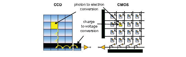
2.12 Comparison readout mode: by charge transfer (CCD), and read directly through the address (CMOS)
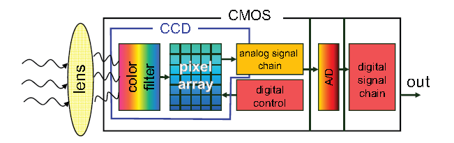
2.13 share the same technology, CMOS sensor and the processing unit may be integrated on a chip, and a CCD sensor and a processing unit must be separated
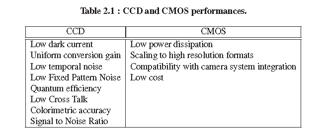
第一个图像sensor诞生于1970,基于CCD(电荷耦合器件)技术。至于COMS传感器,它们是硅基的,材料相似。然而CCD sensor是专门为采集图像而设计的并且发展了40余年。直到几年前,CCD sensor在图像质量这块表现突出,低噪声,高填充因子,高灵敏度和低暗电流(表2.1)。与CMOS(互补金属氧化物半导体)器件不同的是,CCD需要专用的高电压(10V)时钟驱动,高偏置电压(最大15V)和像素按次序读出的缺点,如图2.12。这也迫使开发者分离sensor和图像处理单元(图2.13),由于不同的制造技术(常常sensor和处理单元非同一制造商)从而增加成本,更大的CCD sensor尺寸(结果是需要更大的空间进入设备)。
因上述原因在20世纪90年代末芯片制造商实现了第一款CMOS图像传感器,成像质量差于CCD sensor,因此主要应用于低端市场。然而过去的几年间这一趋势改变了,现在CMOS sensor具有比CCD更高的性价比并且许多专业单反(SLR)中使用CMOS sensor。
CCD和CMOS图像传感器的不同点。
CCD:
l 电荷跨芯片传输并在阵列一角读出;
l 使用特殊制造工艺处理,能不失真跨芯片传输电荷;
l 高填充因子。
CMOS:
l 每个像素对应几个晶体管放大和转移电荷,通过传统的线;
l 更灵活,每个像素能单独读出;
l 高使用同样传统工艺制造主微处理器;
l 集成简单;
l 低填充因子。
图2.12展示了CCD和CMOS不同的读出模式。前者通过按顺序转移像素的值到同列相邻像,直到列末尾。后者可通过实际像素位置寻址直接读出。这意味着CCD sensor中的一个坏点可能会影响整列的读出,而CMOS sensor中只影响它本身值不影响列上其他像素。另外,CCD的读出过程是”按次序的”,因此会慢于CMOS的”并行”通信处理。另外CCD sensor技术和图像信号处理器技术不同,它的尺寸大于同处理器技术一致的CMOS sensor。结果如图2.13,CMOS sensor和处理器可以集成在一起,节省空间,传输问题和电路布局。
3CCD

2.14 3CCD结构器件:输入图像送给3个sensor,1个对应1种颜色sensor
为了获得全彩采集的优势,一些系统使用3个sensor,1个对应一个颜色分量,因此每个像素都可采集其全部颜色分量。使用棱镜将光学系统的输入图像送给sensor。为了图像质量和易于使用,分光棱镜应有几点简单特征:
l 所有输出图像应该面向输入图像同一方向;
l 所有通道光路长度必须相同;
l 棱镜传送所有偏振角度光且均匀性好;
l 保护所有涂层不受环境影响;
l 足够的空间用于装备过滤器和sensor。
这种系统常应用于专业录像机。图2.14展示了一个经典的3CCD采集系统的结构。注意棱镜的设计,使每个sensor实际上处于和镜头相同距离位置。