1. Get to know IIC
IIC (I2C) protocol is a serial communication protocol used to connect microcontrollers and peripheral devices. The IIC protocol only requires two signal lines (clock line SCL and data line SDA) to complete communication between devices; supports multiple hosts and multiple slaves Computer communication, distinguishing different devices throughdevice address; in standard mode, it can reach 100Kbit/s,; has a response mechanism that can detect the correctness of data and the existence of equipment. 3.4Mbit/ sHigh speed mode can reach 400Kbit/s, Fast mode can reach
2. Detailed explanation of the agreement
Inidle state, both the clock line and the data line remainhigh level. The specific transmission process of the IIC protocol is as follows:
1. The host sends the start signal, that is, when the clock line SCL remains high, the data line SDA changes from high to high. Flat to low level transition.
2. The host sends the slave device address and read-write control bit< /span> /span>, that is, when the clock line SCL remains high, the data line SDA Transition from low level to high level. The stop signal indicates the end of an IIC communication. stop signal 6. The host sends signal. The response signal indicates that the host needs to continue receiving data bytes, and the non-response signal indicates that the host has completed receiving or an error has occurred. The non-acknowledge signal is achieved by the host pulling the data line SDA high during the last clock cycle. or non-responsesignal< as neededsends a responsehost, then the host releases the data line SDA and the slave sends the data word Festival. After each byte is received, the read operation 5. If the host sends a signal. If the slave receives the data byte, it pulls the data line SDA low to indicate a response signal. If the slave cannot receive the data byte or an error occurs, then keep the data line SDA high and wait for the master to send a stop signal or a new start signal. host continues to send Data byte, after each byte is sent, the data line SDA is released and waits for the slave's response, then the write operation 4. If the host sends a signal. If there is no match, keep the data line SDA high and wait for the host to send a stop signal or a new start signal. pulls the data line SDA low to indicate the response receives the address and control bits, it performs address recognition. If it matches, it will perform address recognition on the next clock. During the cycle, After the slave machine
3. , the device address of the slave is generally 7 bits, and the read and write control bit is 1 bit, 0 indicates a write operation, and 1 indicates a read operation. After sending the 8-bit data, the master releases the data line SDA and waits for the slave's response signal.
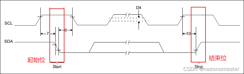
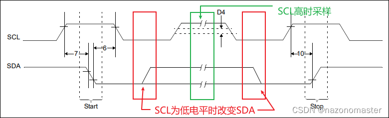
The important start bit and end bit are shown in the figure below, and in the IIC protocol, the device that controls the data line will control the SDA data line whenSCL is low level< /span>:SCL is high level, sample the SDA data line when
3. Specific reading and writing timing
The specific read and write timing diagram is similar to the picture below. This is taken from the manual of a device that supports the IIC protocol. It is worth mentioning that in the picture below, The gray part indicates that the data bus SDA is controlled by the master, and the white part indicates that the data bus SDA is controlled by the slave.
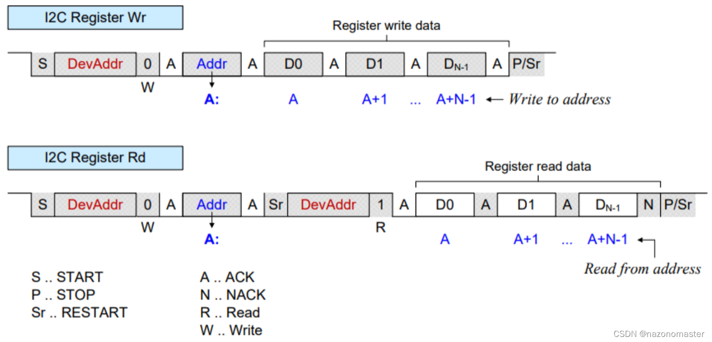
When writing data (I2C Register Wr as shown below): First, the host sends a start bit, followed by a seven-bit wide Device address plus one-bit wide write control bit, slave Response once; then the host sends one byte of register address, from The machine responds once; then the host sends more than one byte of data , the slaveresponds; and finally sends a stop bit.
When reading data (I2C Register Rd as shown below): First, the host sends a start bit, followed by a seven-bit wide Device address plus one-bit wide write control bit; then The master sendsregister address, and the slaveresponds; then resend< /span>non-response. stop bit signal; finally send a . After getting the last byte of data, the host sends a the host responds; the slave machine sends data, responds, used to indicate that the next read operation is to be performed, and the slave machineRead control bit and device address, start bit
4. Design part
Everyone on the website has already explained the design of IIC in great detail. I won’t give a simple explanation here. The following is mainly my personal understanding and design of IIC.
1.Interface design
As a widely used protocol, we should design it into a universal module as much as possible so that it can be used directly next time. Therefore, the interface definition of the module should be as shown in the figure:
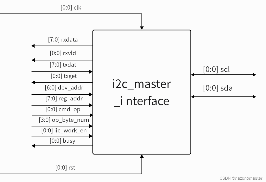
clk Transportation time;
rst is the reset signal (high effective);
txdat indicates the data that needs to be output through IIC;
txget indicates that the signal of this byte has been output;
rxdat represents the data obtained from sda;
rxvld means the data is valid;
dev_addr represents the device address;
reg_addr represents the read and write address (register address);
cmd_op represents a read and write command;
op_byte_num indicates the number of bytes read and written;
iic_work_en indicates the module starts working signal;
busy indicates the working status signal;
scl Display IIC time;
sda Display IIC number;
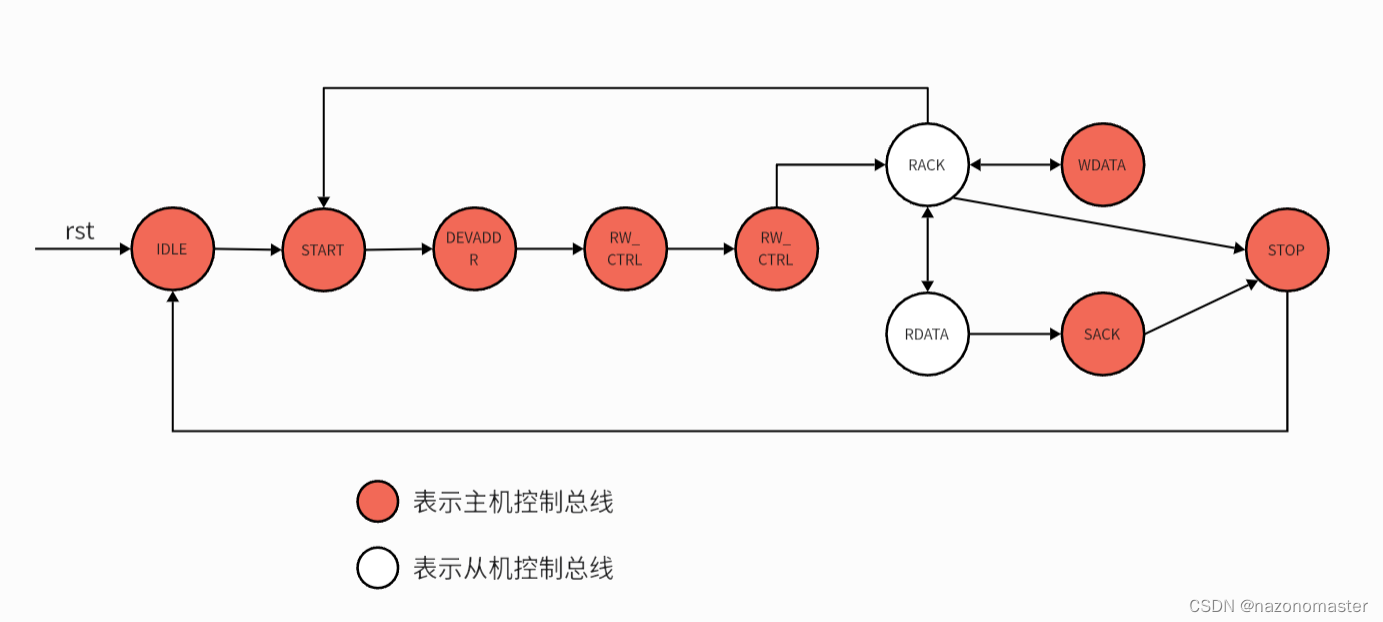
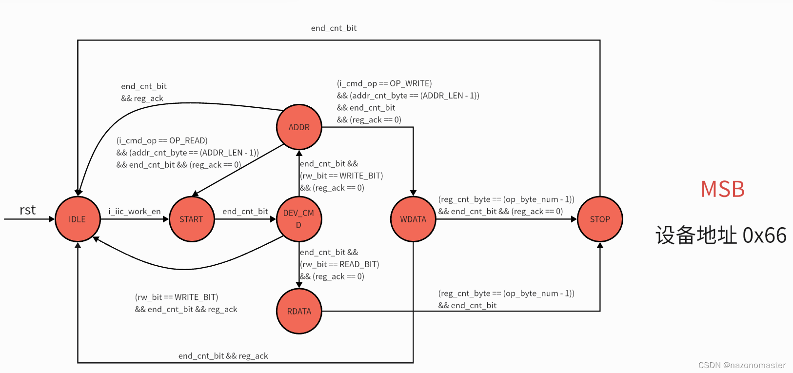
2. State machine design
Because it will be more complicated to make an IIC protocol, the form of a state machine is used here to clarify each operation. But generally the IIC state design we see, including when I designed the IIC before, divides each operation into a state. For example, the start bit is a state, the sending device address is a state, and the read and write control bits are One state, receiving a response and sending a non-response are one state respectively, etc. This division is very detailed, and each operation can be clearly understood at a glance, but I think doing so will make the state jump more complicated, making the entire state The machine becomes very bloated, as shown below.
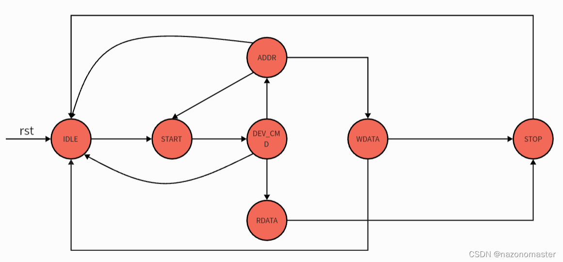
So, I re-conceived the design plan: 9 bits (9bit) are used as one cycle design, that is, every 9 bits or 1 bit is a state. The specific status is as follows:
State 1: IDLE means idle state;
State 2: START represents the starting bit;
State 3: DEV_CMD represents the device address bit, read and write control bit width and the slave’s response bit;
State 4: ADDR represents the address bit of the transmitting register and the response bit of the receiving slave;
Status 5: WDATA represents the write data part;
Status 6: RDATA represents the read data part;
State 7: STOP represents the stop bit;
3. Timing design
writing data timing:
Reading data timing:
4. Code design
First, define the module
Among them, the clock I use is 100Mhz, and the reset signal is active high:
module i2c_master_interface #(
    parameter ADDR_LEN  =   1,
    parameter IIC_CLOCK =   400000
    ) (
    input           i_clk           ,
    input           i_rst           ,

    input   [7:0]   i_txdat         ,
    output          o_txget         ,
    output  [7:0]   o_rxdat         ,
    output          o_rxvld         ,
    input   [6:0]   i_dev_addr      ,
    input [ADDR_LEN*8-1:0] i_reg_addr,
    input           i_cmd_op        ,
    input   [3:0]   i_op_byte_num   ,
    input           i_iic_work_en   ,
    output          o_busy          ,

//output o_output_en,
    inout           io_scl          ,
    inout           io_sda
);


endmodule
The second step is to define the parameters
localparam  SCL_PERIOD  =   1000/(IIC_CLOCK/100000) ,   // in_clk = 100MHz
            SCL_HALF    =   SCL_PERIOD >> 1         ,
            LOW_HALF    =   SCL_HALF >> 1           ,
            HIGH_HALF   =   (SCL_PERIOD+SCL_HALF)>>1;

localparam  IDLE    =   7'b000_0001,
            START   =   7'b000_0010,
            DEV_CMD =   7'b000_0100,
            ADDR    =   7'b000_1000,
            WDATA   =   7'b001_0000,
            RDATA   =   7'b010_0000,
            STOP    =   7'b100_0000;

localparam  WRITE_BIT   =   1'b0,
            READ_BIT    =   1'b1,
            OP_WRITE    =   1'b0,
            OP_READ     =   1'b1;
The third step is to define the signals to be used
reg [6:0]   state_c ;
reg [6:0]   state_n ;

reg [7:0]   cnt_scl ;
reg         reg_scl ;
reg [3:0]   cnt_bit ;
wire        end_cnt_bit;
reg [3:0]   bit_num ;
reg         rw_bit  ;

reg [3:0]   cnt_byte;
reg [3:0]   op_byte_num     ;

reg [ADDR_LEN*8-1:0] reg_addr_1;
reg [7:0]   reg_addr_2      ;

reg [7:0]   reg_txdat       ;
reg         txget           ;

reg         reg_sda         ;
reg         reg_i_sda       ;
reg [7:0]   rx_data         ;
reg         reg_ack         ;
reg         rxvld           ;
reg         busy            ;

wire o_sda;
wire i_sda;
wire o_scl;
wire i_scl;
wire output_en;
The fourth step is to construct a finite state machine
According to logic, the jump conditions of the state machine are as follows:
// FMS
always @(posedge i_clk or posedge i_rst) begin
    if (i_rst) begin
        state_c <= IDLE;
    end
    else begin
        state_c <= state_n;
    end
end

always @(*) begin
    case (state_c)
        IDLE    : begin
            if (i_iic_work_en) begin
                state_n = START;
            end
            else begin
                state_n = state_c;
            end
        end
        START   : begin
            if (end_cnt_bit) begin
                state_n = DEV_CMD;
            end
            else begin
                state_n = state_c;
            end
        end
        DEV_CMD : begin
            if (end_cnt_bit && reg_ack) begin   // NO ACK
                state_n = IDLE;
            end
            else if ((rw_bit == WRITE_BIT) && end_cnt_bit && (reg_ack == 0)) begin   //
                state_n = ADDR;
            end
            else if ((rw_bit == READ_BIT) && end_cnt_bit && (reg_ack == 0)) begin    //
                state_n = RDATA;
            end
            else begin
                state_n = state_c;
            end
        end
        ADDR    : begin
            if (end_cnt_bit && reg_ack) begin
                state_n = IDLE;
            end
            else if ((i_cmd_op == OP_WRITE) && (cnt_byte == (ADDR_LEN - 1)) && end_cnt_bit && (reg_ack == 0)) begin  //
                state_n = WDATA;
            end
            else if ((i_cmd_op == OP_READ) && (cnt_byte == (ADDR_LEN - 1)) && end_cnt_bit && (reg_ack == 0)) begin  //
                state_n = START;
            end
            else begin
                state_n = state_c;
            end
        end
        WDATA   : begin
            if (end_cnt_bit && reg_ack) begin
                state_n = IDLE;
            end
            else if ((cnt_byte == (op_byte_num - 1)) && end_cnt_bit && (reg_ack == 0)) begin  //
                state_n = STOP;
            end
            else begin
                state_n = state_c;
            end
        end
        RDATA   : begin
            if ((cnt_byte == (op_byte_num - 1)) && end_cnt_bit) begin   //
                state_n = STOP;
            end
            else begin
                state_n = state_c;
            end
        end
        STOP    : begin
            if (end_cnt_bit) begin
                state_n = IDLE;
            end
            else begin
                state_n = state_c;
            end
        end
        default: state_n = IDLE;
    endcase
end
The fifth step is to construct intermediate logic
// cnt_bit  bit_num
always @(posedge i_clk or posedge i_rst) begin
    if (i_rst) begin
        cnt_bit <= 0;
    end
    else if ((state_c != IDLE) && (cnt_scl == (SCL_PERIOD - 1))) begin
        if (end_cnt_bit) begin
            cnt_bit <= 0;
        end
        else begin
            cnt_bit <= cnt_bit + 1;
        end
    end
end
assign end_cnt_bit = (state_c != IDLE) && (cnt_scl == (SCL_PERIOD - 1)) && (cnt_bit == (bit_num - 1));

always @(*) begin
    case (state_c)
        IDLE    : bit_num = 0;
        START   : bit_num = 1;
        DEV_CMD : bit_num = 9;
        ADDR    : bit_num = 9;
        WDATA   : bit_num = 9;
        RDATA   : bit_num = 9;
        STOP    : bit_num = 1;
        default : bit_num = 0;
    endcase
end

// rw_bit
always @(posedge i_clk or posedge i_rst) begin
    if (i_rst) begin
        rw_bit <= WRITE_BIT;
    end
    else begin
        case (i_cmd_op)
            OP_WRITE : rw_bit <= WRITE_BIT;
            OP_READ  : begin
                if ((state_c == STOP) && end_cnt_bit) begin
                    rw_bit <= WRITE_BIT;
                end
                else if ((state_c == DEV_CMD) && (rw_bit == WRITE_BIT) && end_cnt_bit && (reg_ack == 0)) begin   //
                    rw_bit <= READ_BIT;
                end
            end
            default  : rw_bit <= rw_bit;
        endcase
    end
end

// cnt_byte  op_byte_num
always @(posedge i_clk or posedge i_rst) begin
    if (i_rst) begin
        cnt_byte <= 0;
    end
    else if (state_c == IDLE) begin
        cnt_byte <= 0;
    end
    else if ((state_c == ADDR) && end_cnt_bit && (reg_ack == 0)) begin
        if (cnt_byte == (ADDR_LEN - 1)) begin
            cnt_byte <= 0;
        end
        else begin
            cnt_byte <= cnt_byte + 1;
        end
    end
    else if ((state_c == RDATA || state_c == WDATA) && end_cnt_bit && (reg_ack == 0)) begin
        if (cnt_byte == (op_byte_num - 1)) begin
            cnt_byte <= 0;
        end
        else begin
            cnt_byte <= cnt_byte + 1;
        end
    end
end

always @(posedge i_clk or posedge i_rst) begin
    if (i_rst) begin
        op_byte_num <= 1;
    end
    else if ((state_c == START) && end_cnt_bit) begin
        op_byte_num <= i_op_byte_num;
    end
end


// reg_addr_1  reg_addr_2
always @(posedge i_clk or posedge i_rst) begin
    if (i_rst) begin
        reg_addr_1 <= 0;
    end
    else if ((state_c == START) && end_cnt_bit) begin
        reg_addr_1 <= i_reg_addr;
    end
end

always @(posedge i_clk or posedge i_rst) begin
    if (i_rst) begin
        reg_addr_2 <= 0;
    end
    else if (state_c == ADDR) begin
        reg_addr_2 <= reg_addr_1[((ADDR_LEN - cnt_byte)*8-1) -: 8];  //
    end
end

// reg_txdat  txget
always @(posedge i_clk or posedge i_rst) begin
    if (i_rst) begin
        reg_txdat <= 8'hff;
    end
    else if (state_c == WDATA) begin
        reg_txdat <= i_txdat;
    end
end

always @(posedge i_clk or posedge i_rst) begin
    if (i_rst) begin
        txget <= 1'b0;
    end
    else if ((state_c == WDATA) && end_cnt_bit) begin
        txget <= 1'b1;
    end
    else begin
        txget <= 1'b0;
    end
end
The sixth step is to build the logic on SCL.
// cnt_scl  reg_scl
always @(posedge i_clk or posedge i_rst) begin
    if (i_rst) begin
        cnt_scl <= 0;
    end
    else if (state_c != IDLE) begin
        if (cnt_scl == (SCL_PERIOD - 1)) begin
            cnt_scl <= 0;
        end
        else begin
            cnt_scl <= cnt_scl + 1;
        end
    end
end

always @(posedge i_clk or posedge i_rst) begin
    if (i_rst) begin
        reg_scl <= 0;
    end
    else if (cnt_scl == SCL_HALF - 1) begin
        reg_scl <= 1;
    end
    else if (cnt_scl == SCL_PERIOD - 1) begin
        reg_scl <= 0;
    end
    else begin
        reg_scl <= reg_scl;
    end
end
The seventh step is to build the logic on SDA
// reg_sda
always @(posedge i_clk or posedge i_rst) begin
    if (i_rst) begin
        reg_sda <= 1'b1;
    end
    else begin
        case (state_c)
            START   : begin
                if (cnt_scl == LOW_HALF - 1) begin
                    reg_sda <= 1'b1;
                end
                else if (cnt_scl == HIGH_HALF -1) begin
                    reg_sda <= 1'b0;
                end
            end
            DEV_CMD : begin
                if (cnt_scl == LOW_HALF - 1) begin
                    case (cnt_bit)
                        0 : reg_sda <= i_dev_addr[6];
                        1 : reg_sda <= i_dev_addr[5];
                        2 : reg_sda <= i_dev_addr[4];
                        3 : reg_sda <= i_dev_addr[3];
                        4 : reg_sda <= i_dev_addr[2];
                        5 : reg_sda <= i_dev_addr[1];
                        6 : reg_sda <= i_dev_addr[0];
                        7 : reg_sda <= rw_bit;
                        default: reg_sda <= reg_sda;
                    endcase
                end
            end
            ADDR    : begin
                if (cnt_scl == LOW_HALF - 1) begin
                    case (cnt_bit)
                        0 : reg_sda <= reg_addr_2[7];
                        1 : reg_sda <= reg_addr_2[6];
                        2 : reg_sda <= reg_addr_2[5];
                        3 : reg_sda <= reg_addr_2[4];
                        4 : reg_sda <= reg_addr_2[3];
                        5 : reg_sda <= reg_addr_2[2];
                        6 : reg_sda <= reg_addr_2[1];
                        7 : reg_sda <= reg_addr_2[0];
                        default: reg_sda <= reg_sda;
                    endcase
                end
            end
            WDATA   : begin
                if (cnt_scl == LOW_HALF - 1) begin
                    case (cnt_bit)
                        0 : reg_sda <= reg_txdat[7];
                        1 : reg_sda <= reg_txdat[6];
                        2 : reg_sda <= reg_txdat[5];
                        3 : reg_sda <= reg_txdat[4];
                        4 : reg_sda <= reg_txdat[3];
                        5 : reg_sda <= reg_txdat[2];
                        6 : reg_sda <= reg_txdat[1];
                        7 : reg_sda <= reg_txdat[0];
                        default: reg_sda <= reg_sda;
                    endcase
                end
            end
            RDATA   : begin     // SACK
                if ((cnt_scl == LOW_HALF - 1) && (cnt_byte == op_byte_num - 1) && (cnt_bit == 8)) begin  //
                    reg_sda <= 1'b1;    // NACK
                end
                else if ((cnt_scl == LOW_HALF - 1) && (cnt_bit == 8)) begin
                    reg_sda <= 1'b0;    // ACK
                end
            end
            STOP    : begin
                if (cnt_scl == LOW_HALF - 1) begin
                    reg_sda <= 1'b0;
                end
                else if (cnt_scl == HIGH_HALF -1) begin
                    reg_sda <= 1'b1;
                end
            end
            default : reg_sda <= reg_sda;
        endcase
    end
end

// reg_i_sda  rx_data  reg_ack  rxvld
always @(posedge i_clk or posedge i_rst) begin
    if (i_rst) begin
        reg_i_sda <= 1'b1;
    end
    else begin
        reg_i_sda <= i_sda;
    end
end

always @(posedge i_clk or posedge i_rst) begin
    if (i_rst) begin
        rx_data <= 0;
    end
    else if ((state_c == RDATA) && (cnt_scl == HIGH_HALF - 1)) begin
        case (cnt_bit)
            0 : rx_data[7] <= reg_i_sda;
            1 : rx_data[6] <= reg_i_sda;
            2 : rx_data[5] <= reg_i_sda;
            3 : rx_data[4] <= reg_i_sda;
            4 : rx_data[3] <= reg_i_sda;
            5 : rx_data[2] <= reg_i_sda;
            6 : rx_data[1] <= reg_i_sda;
            7 : rx_data[0] <= reg_i_sda;
            default: rx_data <= rx_data;
        endcase
    end
end

always @(posedge i_clk or posedge i_rst) begin
    if (i_rst) begin
        reg_ack <= 1'b1;
    end
    else if ((state_c == DEV_CMD || state_c == ADDR || state_c == WDATA) && (cnt_bit == 8) && (cnt_scl == HIGH_HALF -1)) begin
        reg_ack <= reg_i_sda;
    end
end

always @(posedge i_clk or posedge i_rst) begin
    if (i_rst) begin
        rxvld <= 1'b0;
    end
    else if ((state_c == RDATA) && end_cnt_bit) begin
        rxvld <= 1'b1;
    end
    else begin
        rxvld <= 1'b0;
    end
end
Step 8: Construct the busy signal
// busy
always @(posedge i_clk or posedge i_rst) begin
    if (i_rst) begin
        busy <= 1'b0;
    end
    else if (i_iic_work_en) begin
        busy <= 1'b1;
    end
    // else if ((state_c == STOP) && end_cnt_bit) begin
    //     busy <= 1'b0;
    // end
    else if (state_c == IDLE) begin
        busy <= 1'b0;
    end
    else begin
        busy <= 1'b1;
    end
end The ninth step, assignment output
// output
assign o_scl = (state_c == IDLE)? 1 : reg_scl;
assign o_txget = txget;
assign o_rxdat = rx_data;
assign o_rxvld = rxvld;
assign o_busy = busy;
assign o_sda = reg_sda;
assign output_en = (state_c == RDATA)? ((cnt_bit == 8)? 1:0) : ((cnt_bit == 8)? 0:1);

//assign o_output_en = output_en;
The last step is to build the three-state gate
Here we use the primitive IO_BUF in vivado to build:
IOBUF #(
   .DRIVE(12), // Specify the output drive strength
   .IBUF_LOW_PWR("TRUE"),  // Low Power - "TRUE", High Performance = "FALSE"
   .IOSTANDARD("DEFAULT"), // Specify the I/O standard
   .SLEW("SLOW") // Specify the output slew rate
) iobuf_inst_sda (
   .O   (   i_sda   ),     // Buffer output
   .IO  (  io_sda   ),   // Buffer inout port (connect directly to top-level port)
   .I   (   o_sda   ),     // Buffer input
   .T   (~output_en )      // 3-state enable input, high=input, low=output
);

IOBUF #(
   .DRIVE(12), // Specify the output drive strength
   .IBUF_LOW_PWR("TRUE"),  // Low Power - "TRUE", High Performance = "FALSE"
   .IOSTANDARD("DEFAULT"), // Specify the I/O standard
   .SLEW("SLOW") // Specify the output slew rate
) iobuf_inst_scl (
   .O   (   i_scl   ),     // Buffer output
   .IO  (  io_scl   ),   // Buffer inout port (connect directly to top-level port)
   .I   (   o_scl   ),     // Buffer input
   .T   (     0     )      // 3-state enable input, high=input, low=output
);
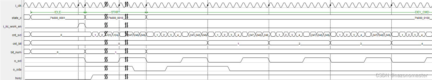
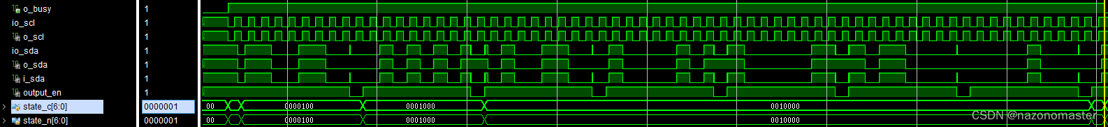
5. Simulation verification
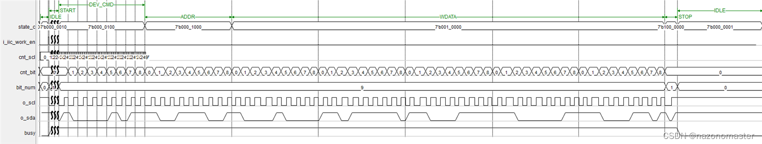
writing timing
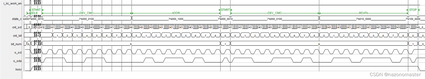
Reading timing:
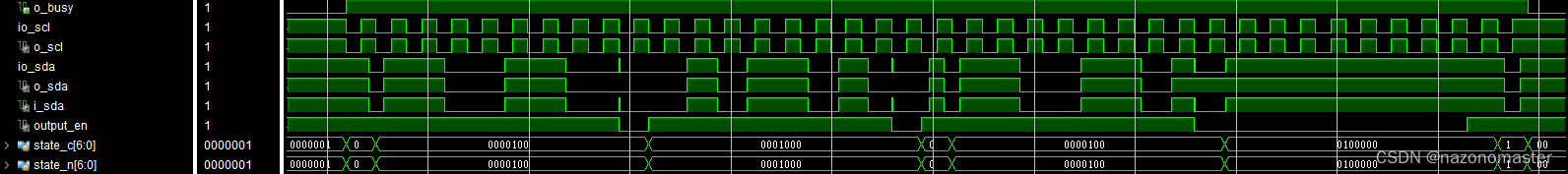
Among them, we can clearly see the following key information:
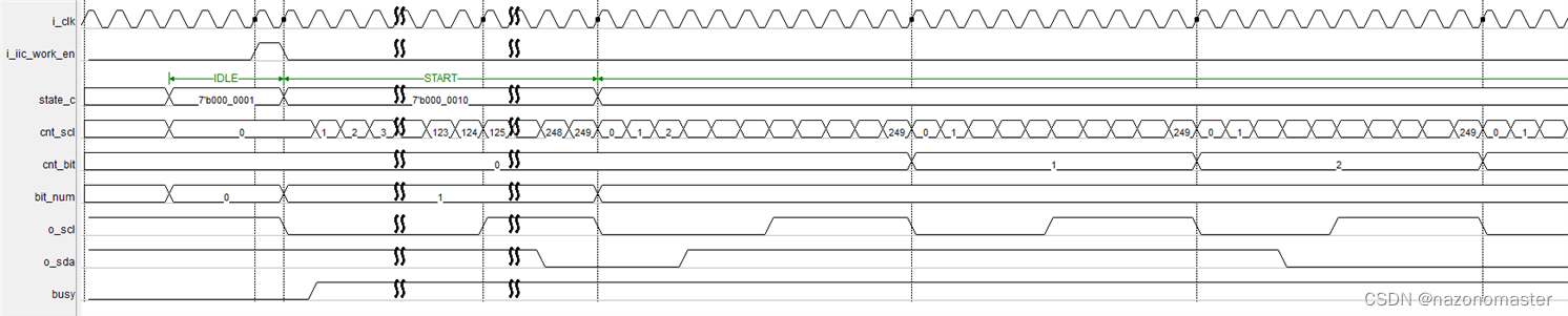
Starting position:

State 2, device address and write control bits:

State 3, sending register address:

Data writing operation, 5 bytes are written:

The RESTART status during the read operation, the device address, the read control bit and the 1-byte data read out:
Stop bit:

5. Description
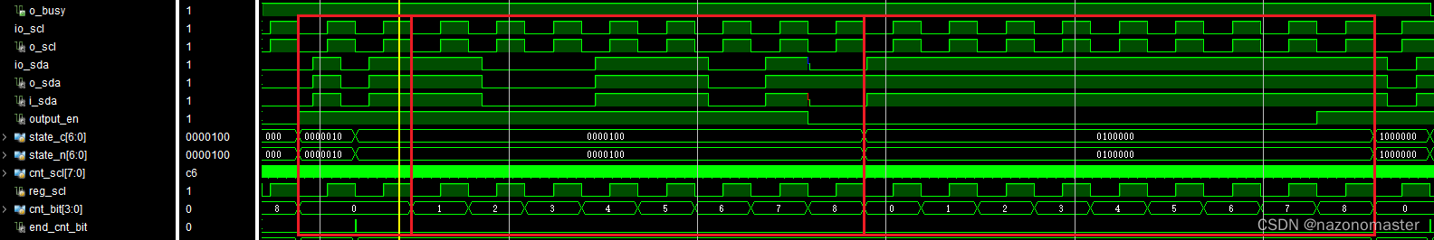
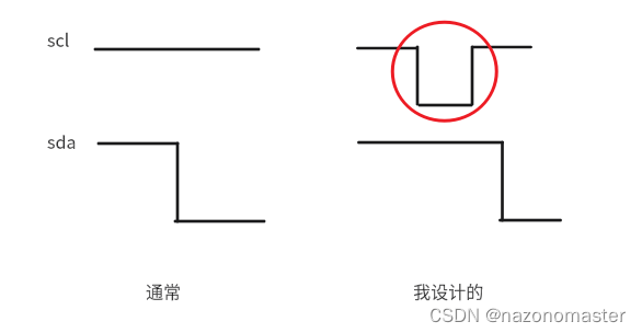
As can be seen from the above design, the SCL I designed goes from low to high. At the same time, when in the start bit state, SCL will also go from low to high. This is consistent with what we usually understand as SCL maintaining at the start bit. The high level does not match, as shown in the figure below:
But after my actual testing on the board, this solution is feasible.
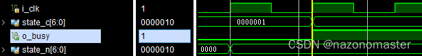
Second point, it can be seen from the above design that due to the influence of sequential logic, the output of the busy signal will be delayed by one cycle compared to the state signal, which means that it is best to use Detect the falling edge of busy to determine whether the IIC interface is still working, or change the assignment logic of the busy signal.