Article directory
Preface
This section describes the simulation and testing of FPGA on-chip RAM. We also know that RAM is random access memory. As the name suggests, it is a module that stores data. When it comes to randomness, that is, we can arbitrarily access some address spaces in it. the data inside.
Xilinx has provided us with the RAM IP core in Vivado. We only need to instantiate a RAM through the IP core and write and read the data stored in the RAM according to the RAM's read and write timing. In the experiment, through the online logic analyzer ila integrated by VIVADO, we can observe the read and write timing of RAM and the data read from RAM.
1. Create and configure projects
1. Create a project
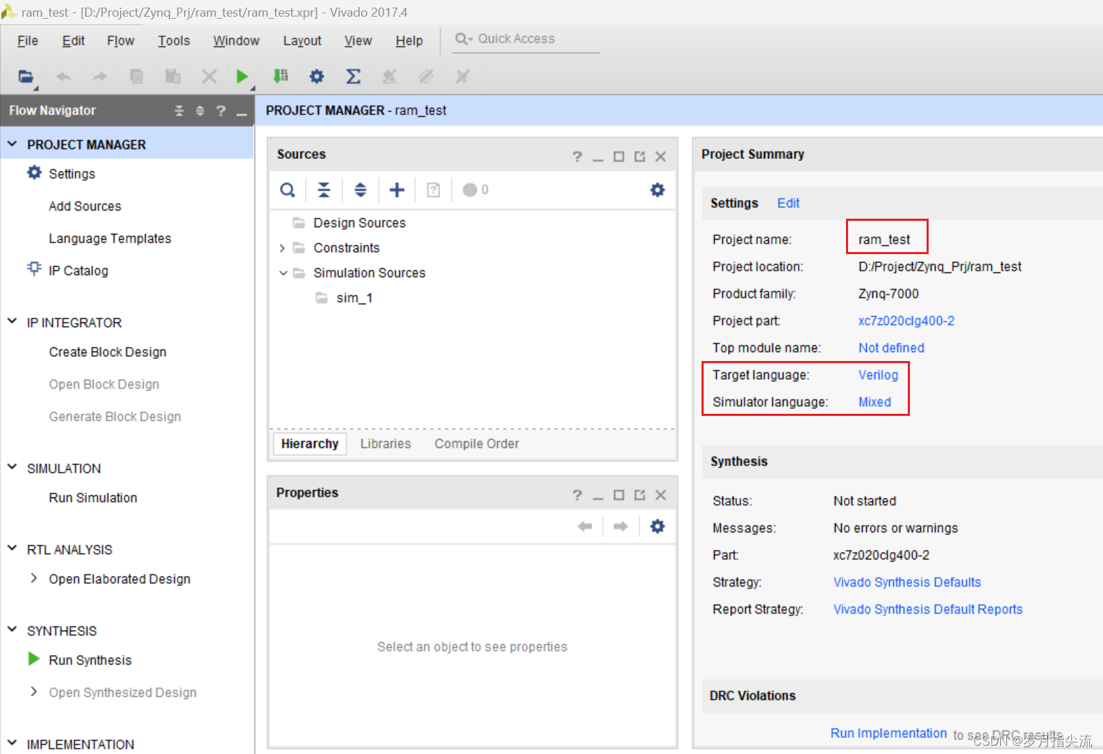
Create a new ram_test project
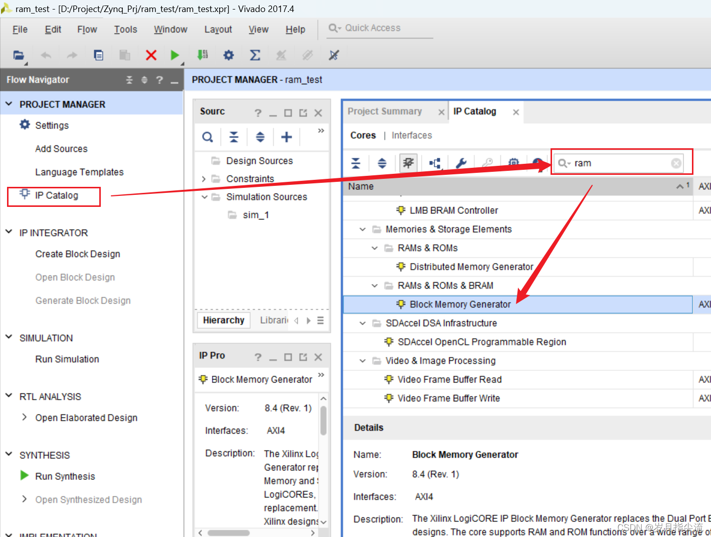
2. Add RAM IP core
①. Click on the IP Catalog in the picture below , search for ram in the interface that pops up on the right, find Block Memory Generator, and double-click to open it.
②. Configure the Basic option bar as shown below.
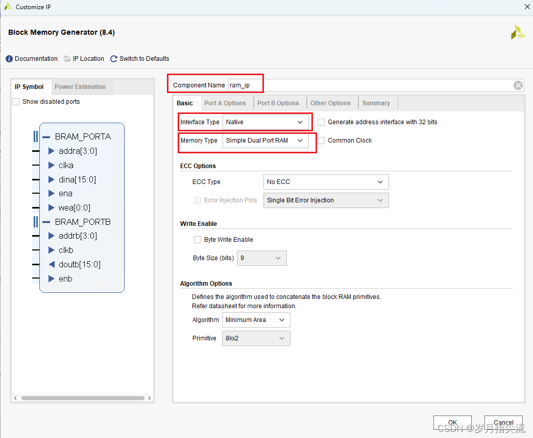
- Interface Type : Interface type, select Native
- There are generally two ways to implement a memory on XILINX's FPGA: the first is to design it yourself using the logic resources of the FPGA; the second is to use XILINX's dedicated Block Memory Generator (BMG) . For BRAM resource forms, XILINX provides two interface types: Native and AXI4. The main characteristics of these two cores are as follows.

- There are generally two ways to implement a memory on XILINX's FPGA: the first is to design it yourself using the logic resources of the FPGA; the second is to use XILINX's dedicated Block Memory Generator (BMG) . For BRAM resource forms, XILINX provides two interface types: Native and AXI4. The main characteristics of these two cores are as follows.
- Memory Type: Memory type, select Simple Dual Port RAM
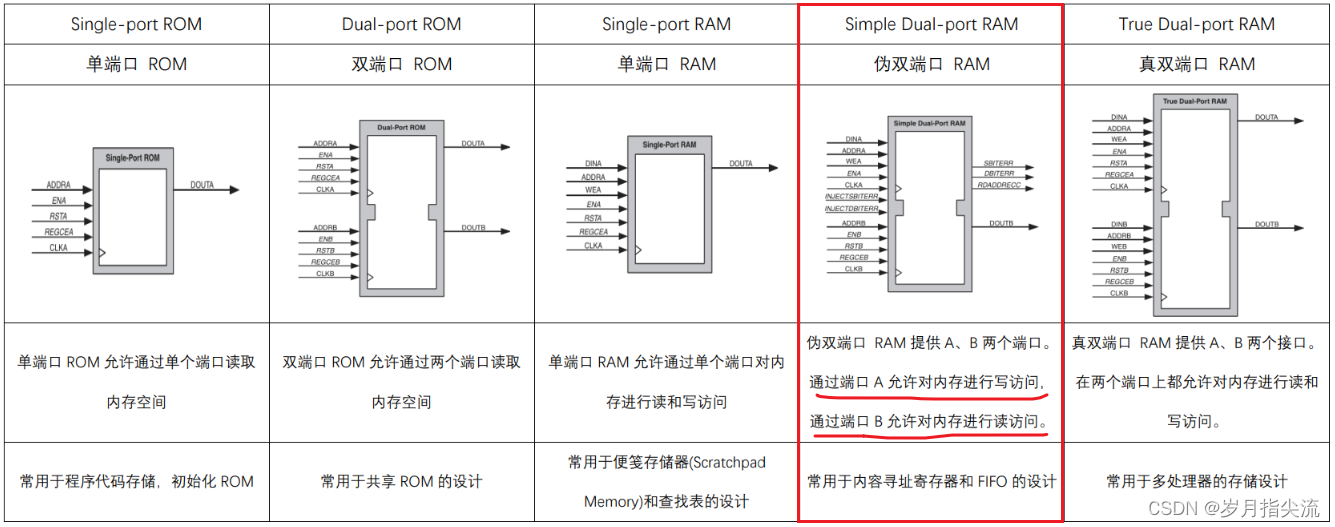
- There are five memory types of the Native port. The differences are as follows:
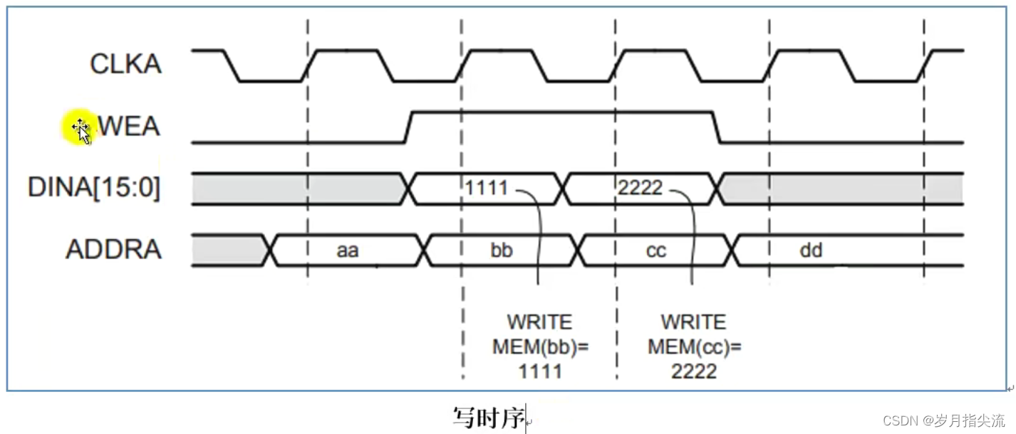
- The write timing of Simple Dual Port RAM is as follows
- When the write enable is valid (high level), the specified data is written to the specified address on the rising edge of the clock.
- When the write enable is valid (high level), the specified data is written to the specified address on the rising edge of the clock.
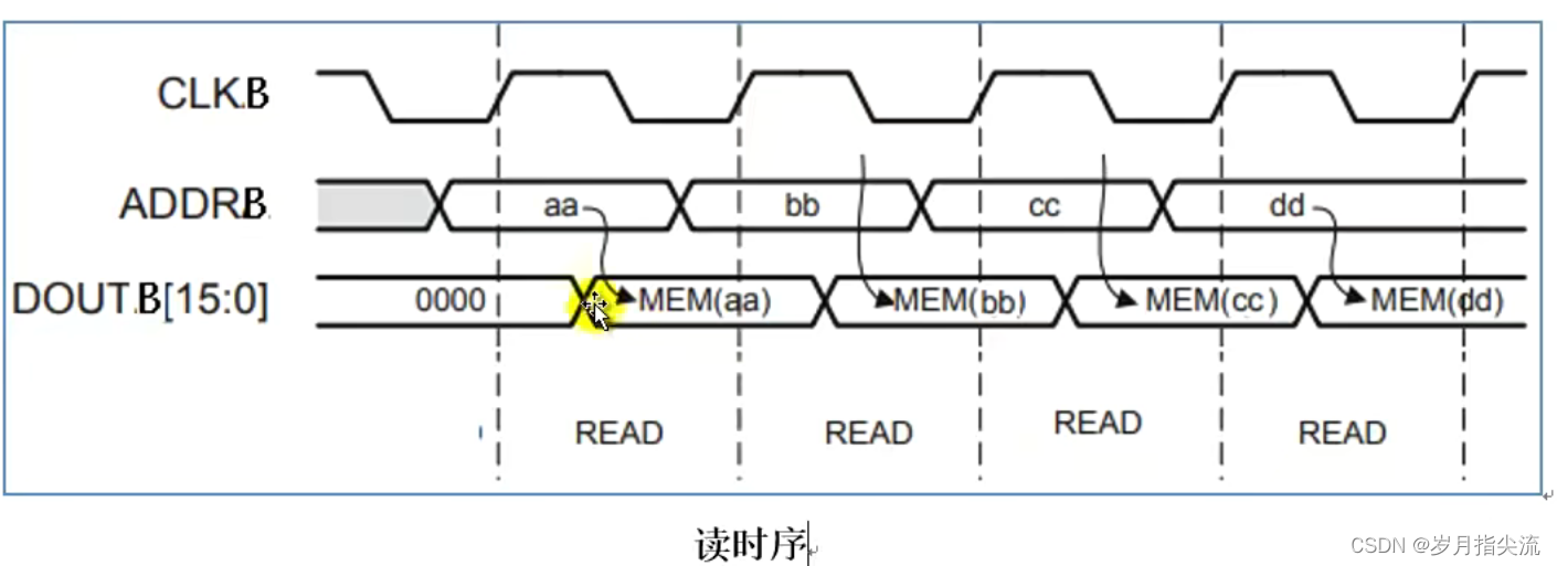
- The read timing of Simple Dual Port RAM is as follows
- There is a certain delay when reading. If we collect this valid output data at the same clock, we need to collect its valid data in the next cycle.
- There is a certain delay when reading. If we collect this valid output data at the same clock, we need to collect its valid data in the next cycle.
- There are five memory types of the Native port. The differences are as follows:
③. Configure the Port A Option option bar as shown below.
按照这样设置,也就是说可以存储 512 个 16 位数据
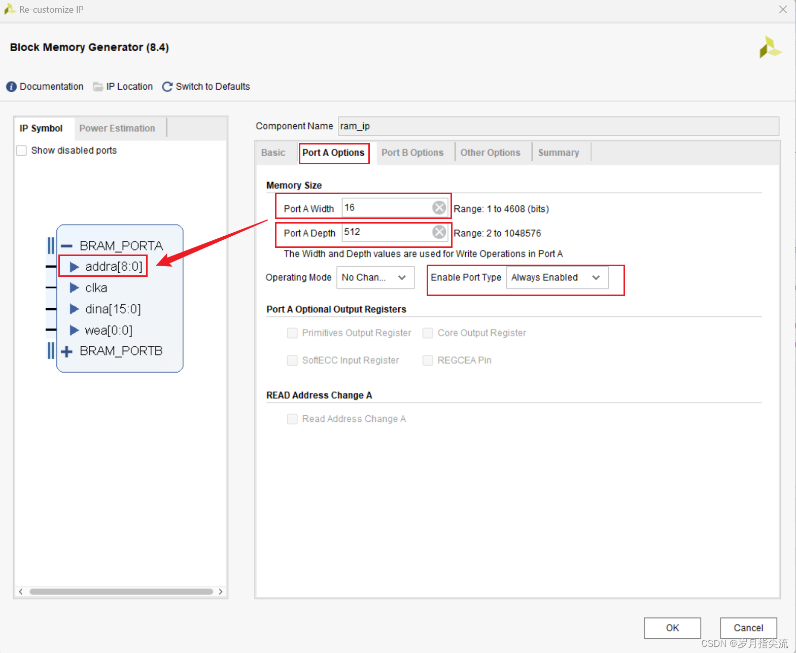
- Port A Width (data width): the width of port A, here we set 16 bits wide
- Port A Depth (how much data can be stored in RAM): the depth of port A, we set it here to 512
- Enable Port Type: Always Enable, keep it enabled so we don’t need to control it
④. Configure the Port B Option option bar as shown below.
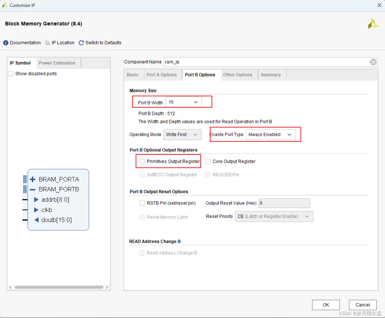
- Port B Width (data width): the width of port B, here we set 16 bits wide
- Enable Port Type: Always Enable (the enable of port B remains on)
- Primitives Output Register: Uncheck, its function is to add a register to the output data, which can effectively improve the timing, but the read data will lag behind the address by two cycles . In many cases, this function is not enabled and the data is kept one cycle behind the address.
For more information on other settings, please refer to XILINX's official document " Block Memory Generator v8.4 LogiCORE IP Product Guide "
⑤. Other Options, just keep the default configuration.
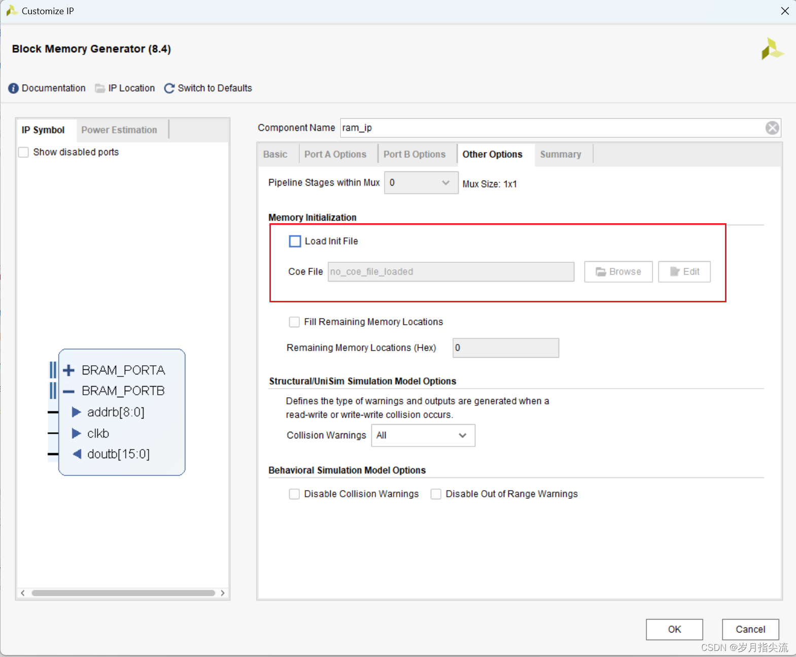
- Load Init File allows us to initialize some files and put them in RAM, which means that after the FPGA is powered on, it will load the data you have saved in advance into RAM.
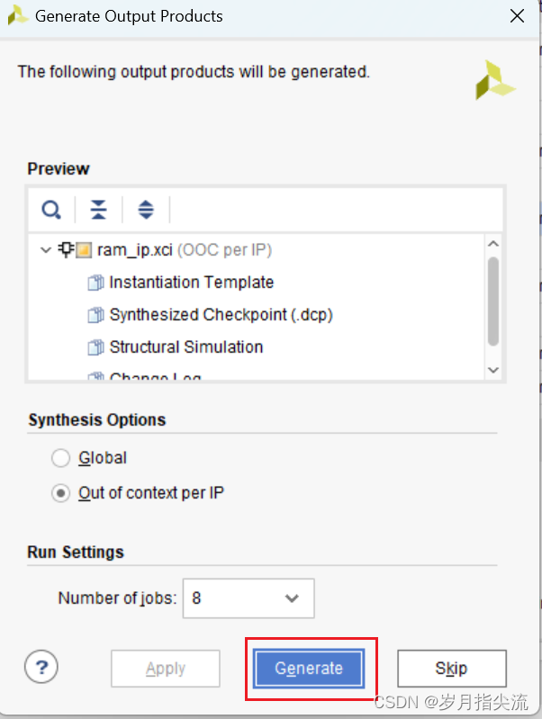
⑥. Click OK, then click Generate to generate the RAM IP
3. Add ILA IP core
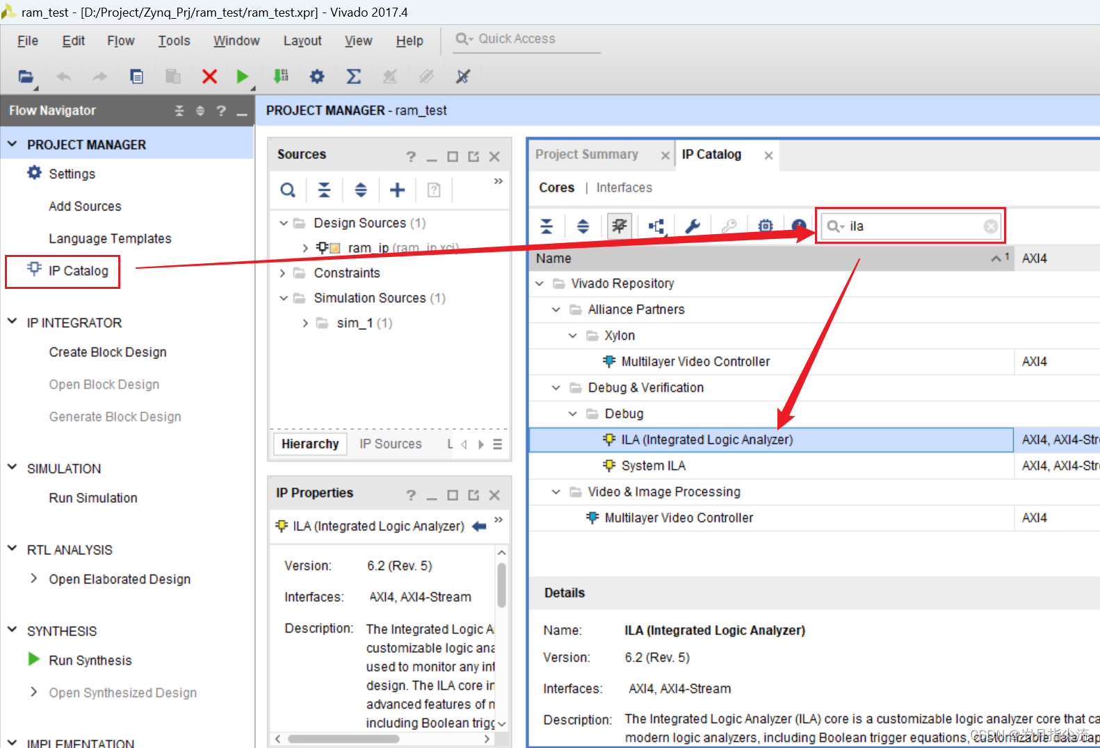
①. Click on the PROJECT MANAGER bar on the left -> IP Catalog or Window -> IP Catalog under the menu bar, then search for ILA under the IP Catalog window that appears on the right, double-click to select ILA under Debug for IP configuration. The steps are as shown in the figure below
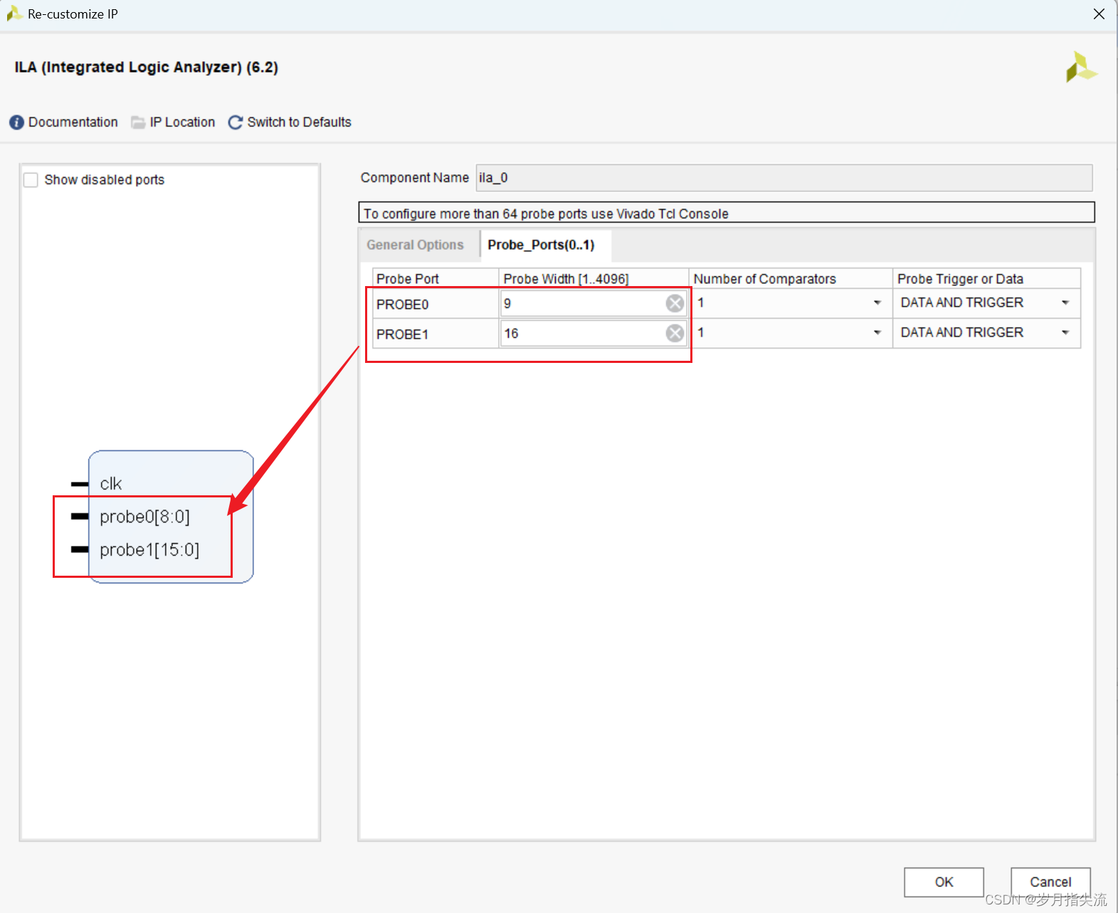
② , General Option adds two probes to collect the address and data we read. We set the length of the sampled data larger, as shown in the figure below
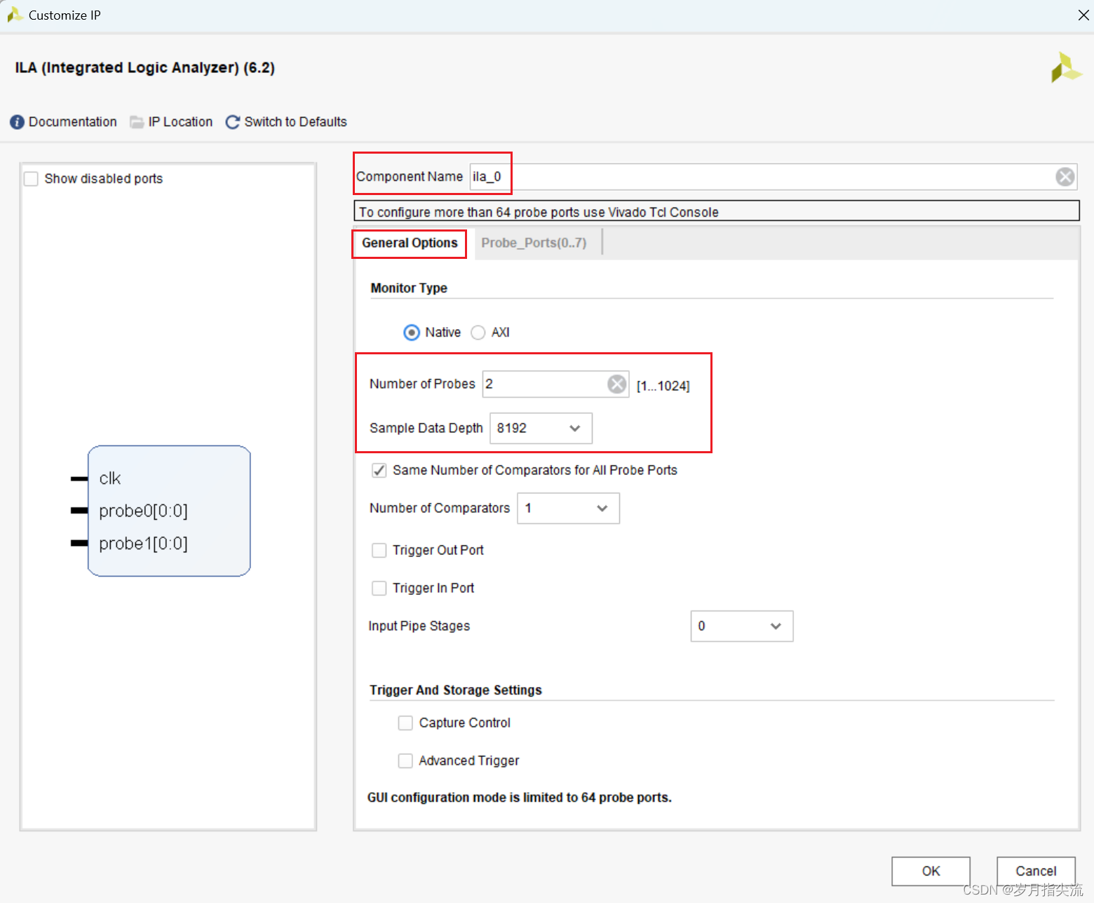
③. PROBE0 in Probe_Ports (0...7) is used to collect the 9-bit address, and PROBE1 is used Collect 16-bit data, as shown in the figure below
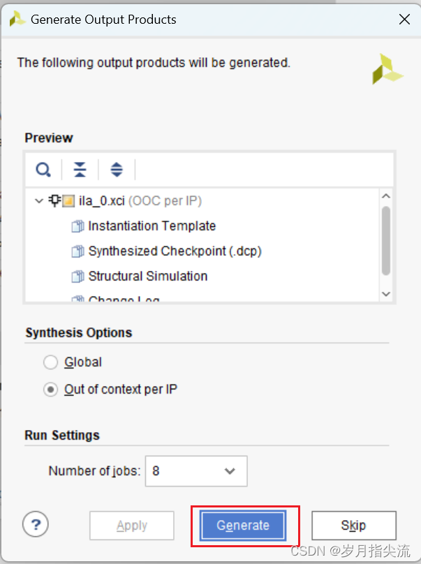
④, click OK, and then click Generate to generate ILA IP
2. Programming
Before writing the program, let’s first introduce what signals we involve
Simple Dual Port RAM module port descriptions are as follows:
| Signal name | direction | illustrate |
|---|---|---|
| clka | in | Port A clock input |
| wea | in | Port A enabled |
| addra | in | Port A address input |
| ignoble | in | Port A data input |
| clkb | in | Port B clock input |
| addrb | in | Port B address input |
| doutb | out | Port B data output |
The data writing and reading of RAM are operated on the rising edge of the clock. When writing data to port A, the wea signal needs to be set high, and the address and data to be written need to be provided at the same time. The figure below shows the timing diagram of input writing to RAM.
Port B cannot write data and can only read data from RAM. As long as the address is provided, valid data can generally be collected in the next cycle.
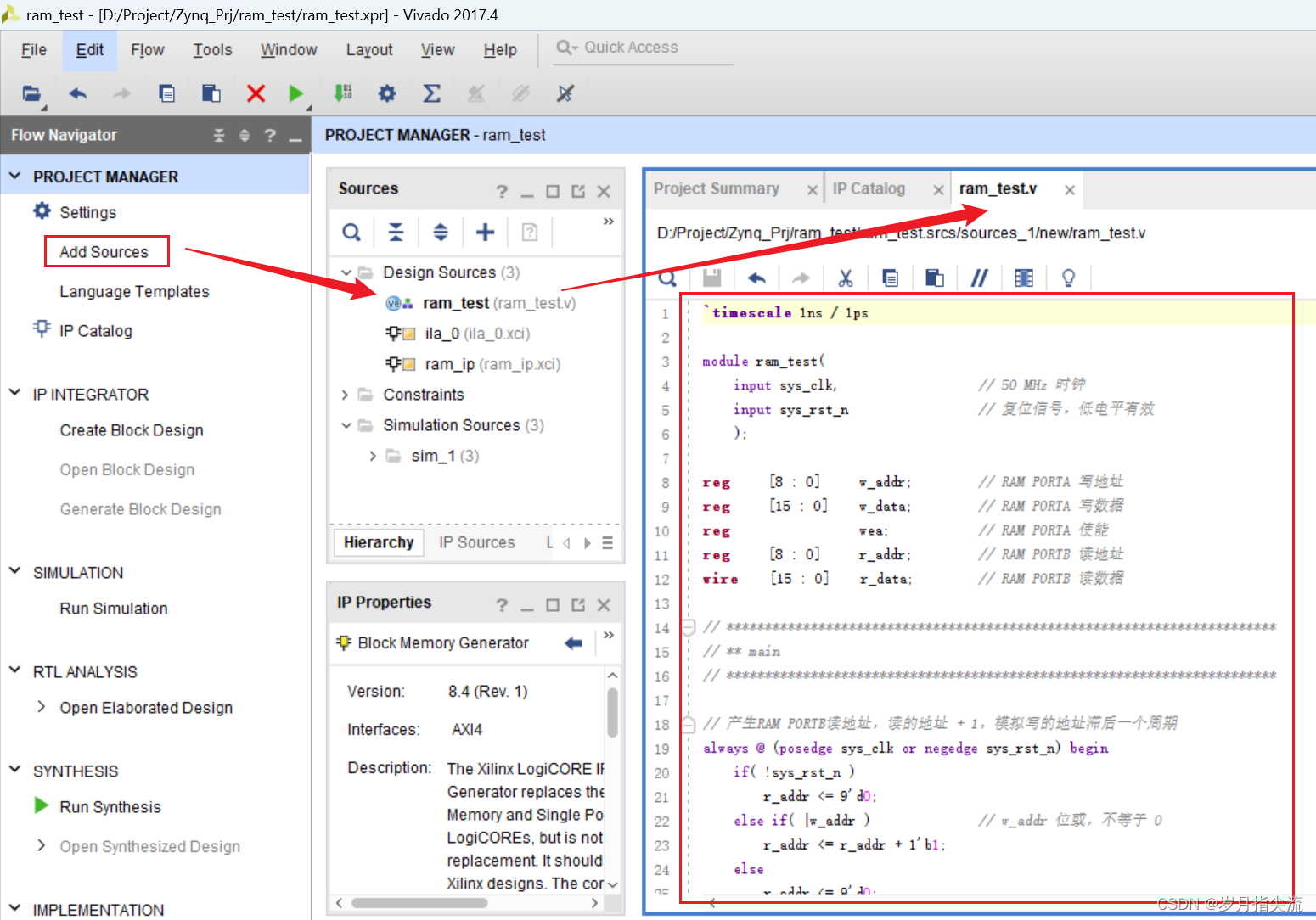
1. Create a new test program
Create a new ram_test.v source file and copy the following program blocks to
ram_test.v
`timescale 1ns / 1ps

module ram_test(
    input clk,					// 50 MHz 时钟
    input rst_n					// 复位信号,低电平有效
    );

reg     [8 : 0]     w_addr;			// RAM PORTA 写地址
reg     [15 : 0]    w_data;			// RAM PORTA 写数据
reg                 wea;			// RAM PORTA 使能
reg     [8 : 0]     r_addr;			// RAM PORTB 读地址
wire    [15 : 0]    r_data;			// RAM PORTB 读数据

// ************************************************************************
// ** main
// ************************************************************************

// 产生RAM PORTB读地址,读的地址 + 1,模拟写的地址滞后一个周期
always @ (posedge clk or negedge rst_n) begin
    if( !rst_n )
        r_addr <= 9'd0;
    else if( |w_addr )				// w_addr 位或,不等于 0
        r_addr <= r_addr + 1'b1;
    else
        r_addr <= 9'd0;
end

// 产生RAM PORTA写使能信号
always @ (posedge clk or negedge rst_n) begin
    if( !rst_n )
        wea <= 1'b0;
    else begin
        if( &w_addr )				// w_addr 的 bit 位全为1,共写 512 个数据,写入完成
            wea <= 1'b0;
        else
            wea <= 1'b1;			// ram 写使能
    end
end

// 产生RAM PORTA写入的地址及数据
always @ (posedge clk or negedge rst_n) begin
    if( !rst_n ) begin
        w_addr <= 9'd0;
        w_data <= 16'd1;
    end
    else begin
        if( wea ) begin				// ram 写使能有效
            if( &w_addr ) begin		// w_addr 的 bit 位全为 1,共写入 512 个数据,写入完成
                w_addr <= w_addr;	// 将地址和数据的值保持住,只写一次 RAM
                w_data <= w_data;
            end
            else begin
                w_addr <= w_addr + 1'b1;
                w_data <= w_data + 1'b1;
            end
        end
    end
end

// 实例化 RAM
ram_ip ram_ip_instance (
  .clka(clk		),			// input wire clka
  .wea(wea			),      // input wire [0 : 0] wea
  .addra(w_addr		),  	// input wire [8 : 0] addra
  .dina(w_data		),    	// input wire [15 : 0] dina
  .clkb(clk		),    		// input wire clkb
  .addrb(r_addr		),  	// input wire [8 : 0] addrb
  .doutb(r_data		)  		// output wire [15 : 0] doutb
);

// 实例化 ila 逻辑分析仪
ila_0 ila_0_instance (
	.clk(clk), 				// input wire clk
	.probe0(r_addr), 		// input wire [8:0]  probe0
	.probe1(r_data) 		// input wire [15:0]  probe1
);

endmodule
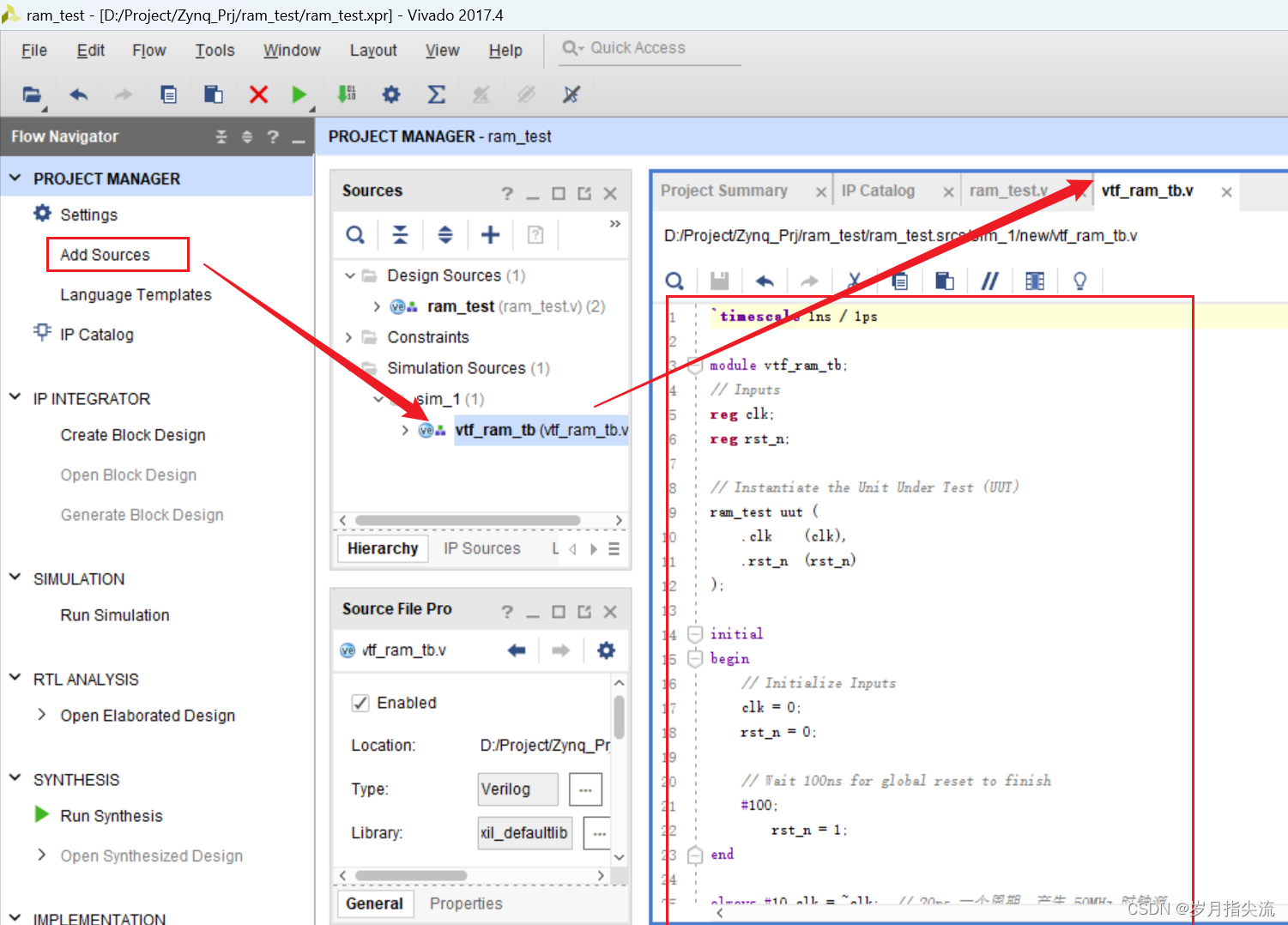
2. Create a new simulation file
Create a new vtf_ram_tb.v simulation file and copy the following program blocks to
vtf_ram_tb.v
`timescale 1ns / 1ps

module vtf_ram_tb;
// Inputs
reg clk;
reg rst_n;

// Instantiate the Unit Under Test (UUT)
ram_test uut (
	.clk 	(clk),
	.rst_n 	(rst_n)
);

initial
begin
	// Initialize Inputs
	clk = 0;
	rst_n = 0;

	// Wait 100ns for global reset to finish
	#100;
		rst_n = 1;
end

always #10 clk = ~clk;	// 20ns 一个周期,产生 50MHz 时钟源

endmodule
3. Carry out simulation
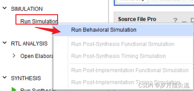
①. Click Run Simulation -> Run Behavioral Simulation to perform simulation
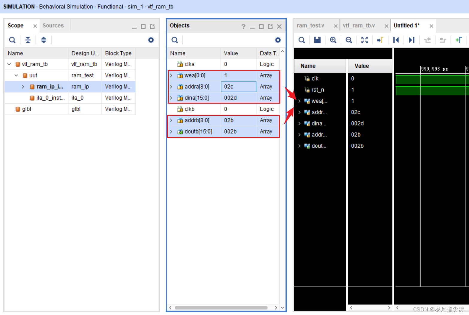
②. Drag the relevant signals in RAM into the observation window
(clocka and clockb use the system clock, so there is no need to drag it into the observation window here)
③. Set a 200us run Next
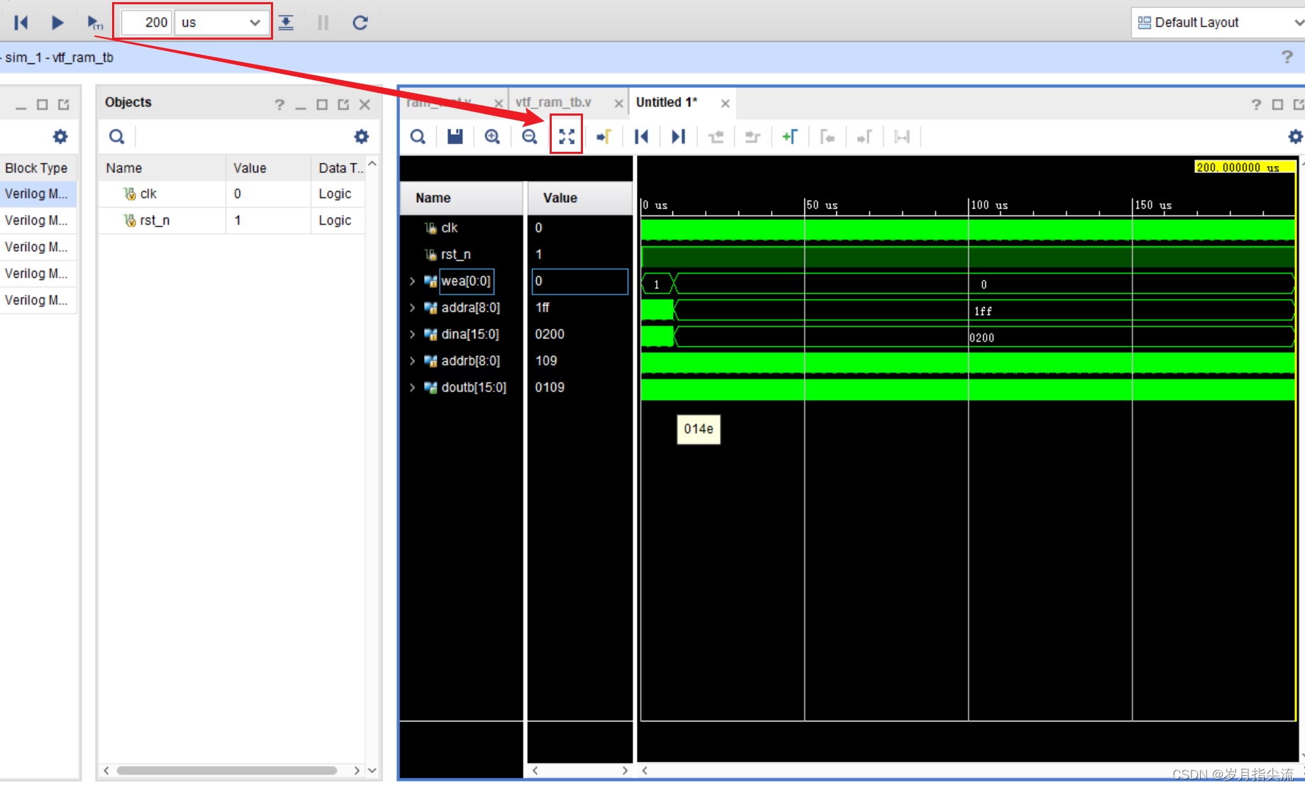
④, analyze the waveform
The starting waveform information
can be seen that the read address lags behind the write address by one clock cycle, and the read data is
the waveform information that lags behind the end of the write address by one clock cycle.
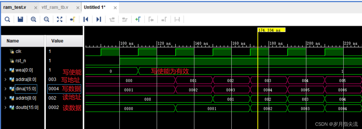
Here we view these signals in decimal form.
You can see that the last address written is 511, the content written is 512, the last address read is 511, and the content read is 512. You
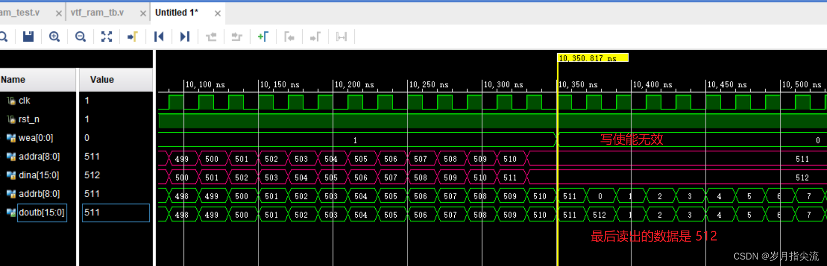
can find that our writing only writes first, while reading is always going on.
4. Download to FPGA
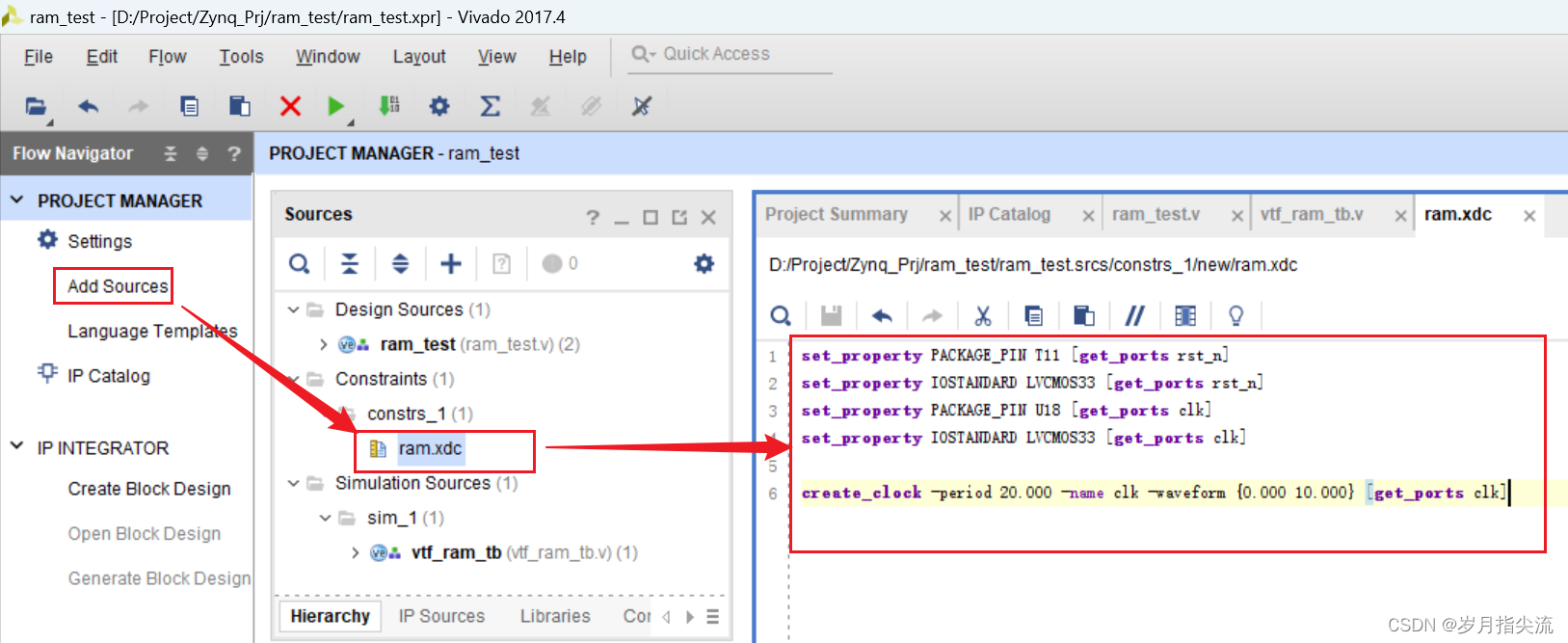
1. Pin constraints and timing constraints
rst_n -> T11
clk -> U18
Create a new pin constraint file ram.xdc, copy the following statements and save it
set_property PACKAGE_PIN T11 [get_ports rst_n]
set_property IOSTANDARD LVCMOS33 [get_ports rst_n]
set_property PACKAGE_PIN U18 [get_ports clk]
set_property IOSTANDARD LVCMOS33 [get_ports clk]

create_clock -period 20.000 -name clk -waveform {

    0.000 10.000} [get_ports clk]
2. Generate bit file
Click "Generate Bitstream" to directly generate the bit file
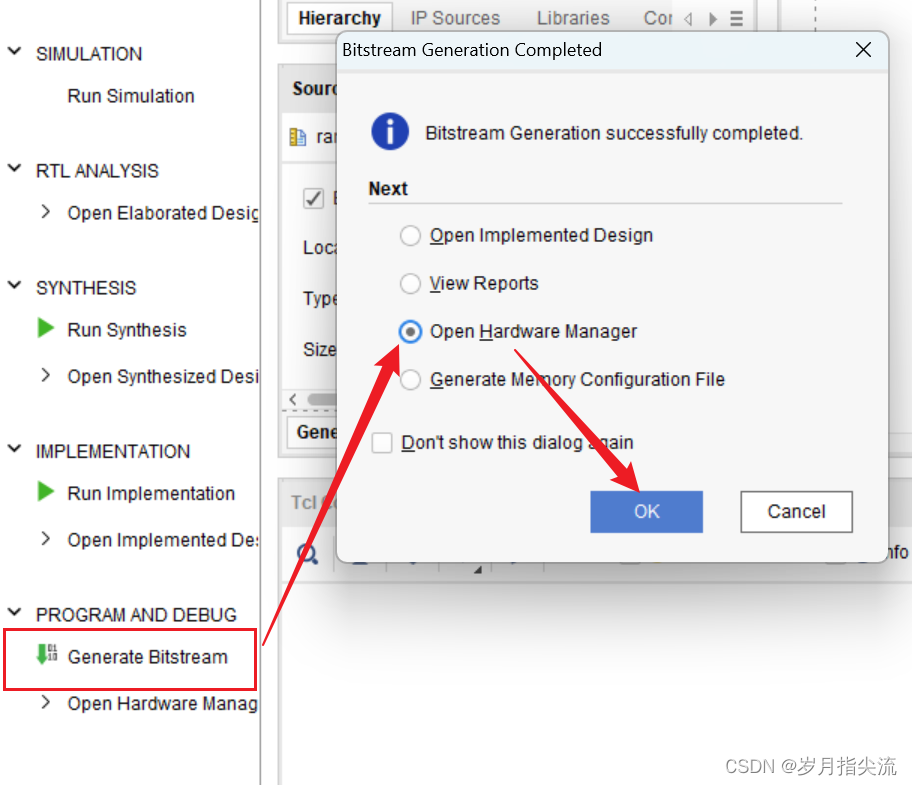
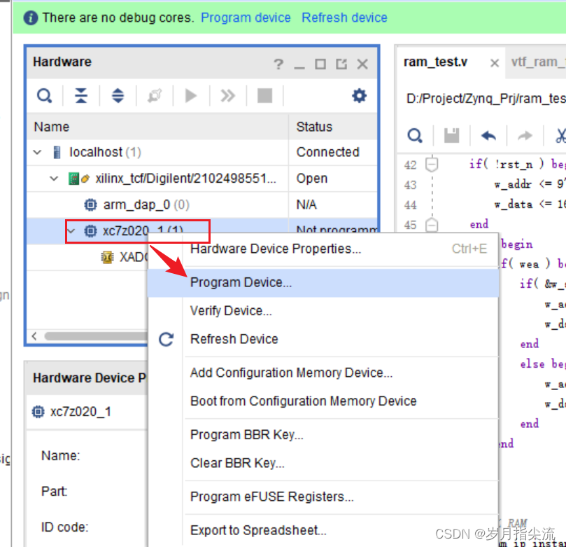
3. Download the program
Connect the JTAG and power cable, power on the board, and download the program
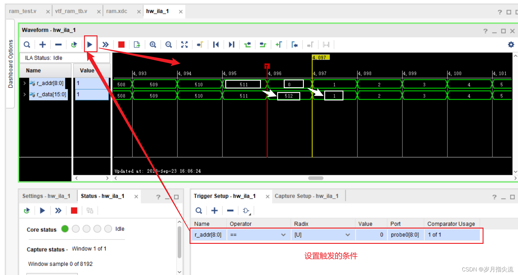
4. Logic analyzer analyzes waveforms
View the read memory and data in decimal mode, set the trigger condition to "the read address is 0", you can see that the data read at address 0 is 1, and the data read at address 511 is 512. It can be seen that the conditions are met the expected results.
5. Obtain resources by yourself
FPGA on-chip RAM read and write test experiment
My qq: 2442391036, welcome to communicate!