SDRAM:
Synchronous Dynamic Random Access Memory
Synchronous Dynamic RAM Transfer
Advantages: large storage capacity,
Fast reading and writing speed,
relatively cheap
Disadvantages: complex control logic

So my size is: 4 x 2^13 x 2^9 x 16 = 268435456 bit = 262144 kbit = 256Mbit = 32M b
SDRAM initialization:
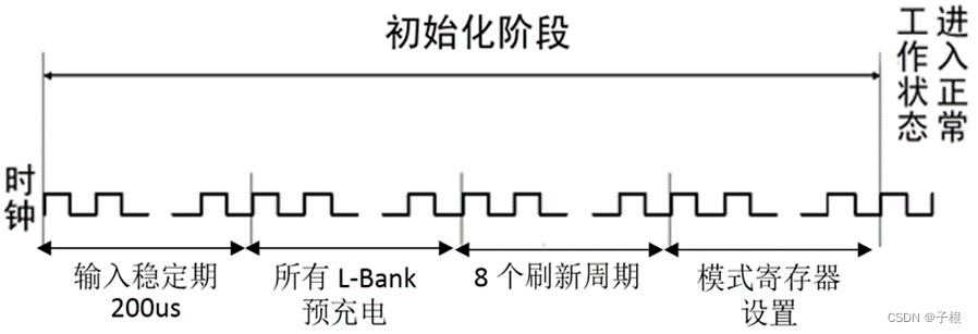
1.200us stable period
2. L-Bank pre-charge
3.8 refreshes
4. Register setting
Register Settings (MRS)
Mode Register Set Cycle ( tRSC )
It takes a while to set the register
SDRAM read and write:
Line activation:
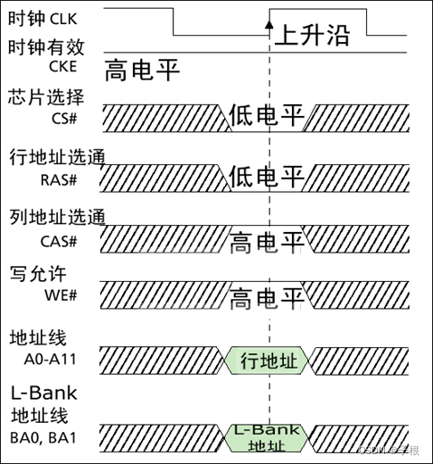
CKE is active high
# means low level active
The "chip selection" of the SDRAM chip and the "addressing" of the L-Bank are performed simultaneously with the row activation
CKE: 1
CS#: 0
RAS#: 0
CAS#: 1
WE#: 1
A0-A11: row address
L_Bank: bank address
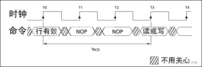
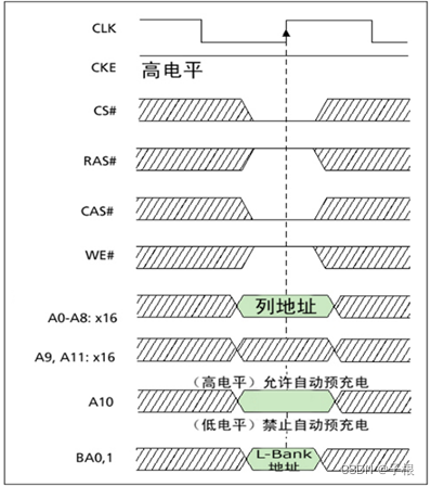
Column read and write:
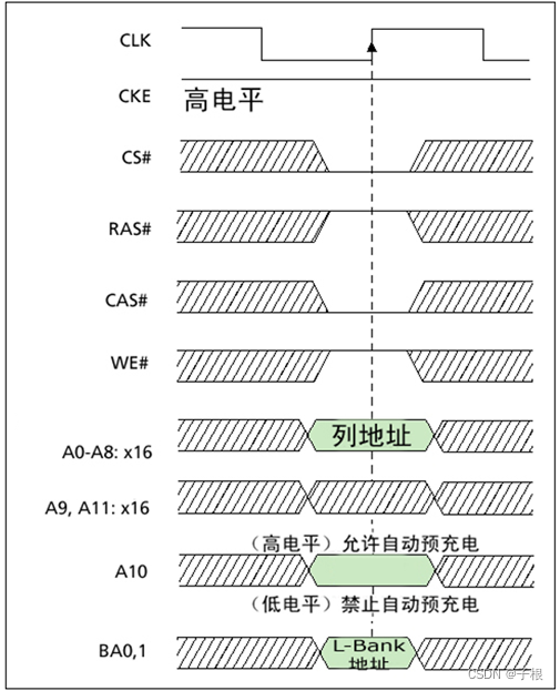
CKE: 1
CS#: 0
RAS#: 1
CAS#: 0
WE#: 1
A0-A8: column address
L_Bank: bank address
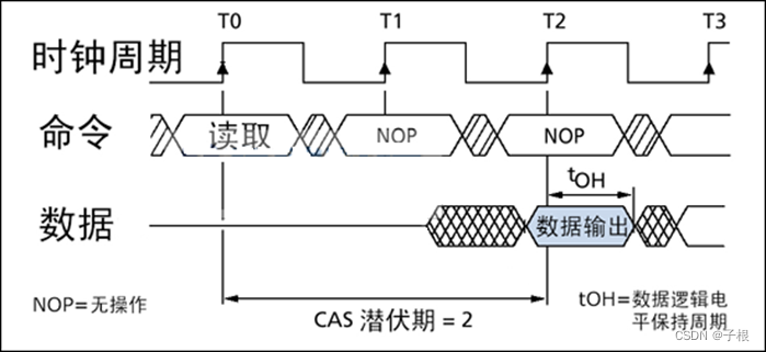
data readout
After the column address is sent, it takes a latency period before the data is output
Data written out:

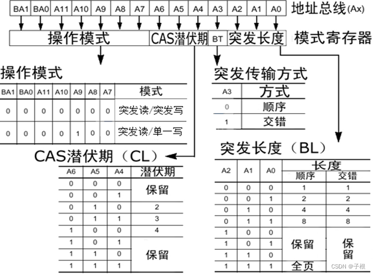
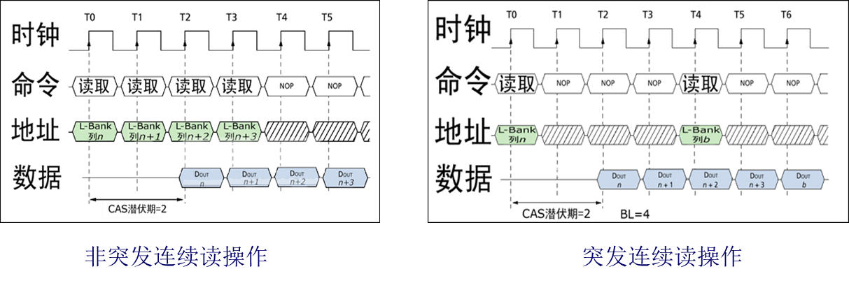
burst length
Burst ( Burst ) refers to the method of continuous data transmission between adjacent storage units in the same row. The number of storage units (columns) involved in continuous transmission is the burst length (Burst Lengths, BL for short ) .
data mask
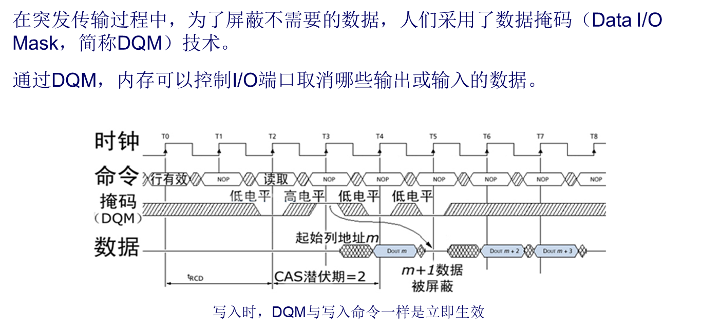
DQM is active at high level and can only mask 8-bit data at a time.
Precharge:
Close this line, open the next line
to refresh
The reason why SDRAM is called synchronous "dynamic" random access memory is because it needs to be refreshed continuously ( Refresh ) to retain data, so refreshing is the most important operation of SDRAM .
Generally, it is refreshed at least 60ms. The main purpose of refreshing is to prevent power failure and data loss for previous lines.