Table of contents
1. Basic knowledge of microcontroller
2. Microcontroller structure and principle
(3) Special function register (SFR)
(4) Differences between MCS-51 products
1. Basic knowledge of microcontroller
(1) Number system and coding
- Binary original code, complement code, complement code
Original code The first sign bit; the other bits are numerical bits (1 negative, 0 positive) A positive number The original code, inverse code and complement code are all the same negative number The complement code is "the sign bit is 1, and the numerical bit is inverted bit by bit" ; the complement code is +1 at the end of the complement code" - The 4 digits of the BCD code only represent 0~9 (exceeding 9 will be represented separately, please note that it is different from binary)
(2) Memory introduction
- The basic circuit components of a computer : commonly used logic circuits (AND, OR, NOT, XOR, NAND, NOR, etc.); registers (composed of flip-flops, common ones include buffer registers, shift registers, counters, etc.)
- Commonly used terms in memory :
| storage unit | Composed of a large number of buffer registers, one register is called a storage unit |
| bit |
The smallest unit of data in a computer is a binary bit |
| Word length (bit length) |
The number of digits in the code generally refers to the number of operands involved in an operation. |
| Byte | An 8-bit binary code is a byte |
| capacity unit | The maximum number of storage cells that a piece of memory can accommodate. Common capacity units: KB (1KB=1024B), MB (1MB=1024KB), GB (1GB Gigabit=1024MB) |
- MCU processing functions: byte processing (overall assignment); bit processing (single assignment)
- Main semiconductor memories:
ROM (read only memory) Store fixed programs and will not be lost when the power is off RAM (random access memory) Store data and frequently changed programs, random storage will be lost when power is off - Storage unit and storage address : The storage address is a unique fixed number of the storage unit
- Number of storage units and address lines : n wires can be translated into 2^n address numbers (that is, there can be 2^n storage units)

2. Microcontroller structure and principle
(1) Microcontroller structure
- Level: MCU - MCU system - MCU application system
- The number of digits of the microcontroller: 8, 16, and 32 bits refer to the "word length" of the microcontroller, that is, the length of data involved in an operation. This bit refers to the binary bit. The number of bits in a microcontroller is closely related to performance. Usually the order of performance is 32 bits > 16 bits > 8 bits.
| Number of digits in microcontroller | Representation range | Detailed explanation |
|---|---|---|
| 8-bit (MCS-51) | 0~255D | The maximum number of data involved in each operation cannot exceed 255 |
| 16 bit | 0~65535D | The maximum number of data involved in each operation cannot exceed 65535. |
| 32 bit | 0~4294967295D | The maximum data involved in each operation cannot exceed 4294967295 |
- The composition of a standard microcontroller
| Basic components of microcontroller | Specific composition (main components) | function, address space |
|---|---|---|
| Central processing unit (CPU) | Central processing unit (PC, ALU, instruction register, etc.) with a word length of 8 bits | operation, control |
| Program memory (internal ROM) | Store programs and fixed constants | 4KB/8KB flash memory |
| Data memory (internal RAM) | Store changed data (special registers are placed in internal RAM) | for 256 RAM cells |
| Timer/Counter | Timing and counting functions | |
| Parallel I/O port | Realizes parallel input/output of data in external devices, and some pins have taking functions | 4 8-bit I/O ports |
| Serial port | Realize asynchronous serial data transfer between microcontroller and other devices with corresponding interfaces | UART full-duplex asynchronous serial port; ISP serial interface |
| Clock circuit | Generate the clock pulse sequence (oscillator, timing, control circuit) required for microcontroller operation | Requires external crystal oscillator and trimmer capacitor |
| interrupt system | Manage and process external or internal interrupt requests | External interrupt/internal interrupt/timer interrupt |
| bus controller | When the microcontroller needs to expand the peripheral interface chip, it is used to control the addressing and data transmission of the external chip. |
- Microcontroller pins (40x):
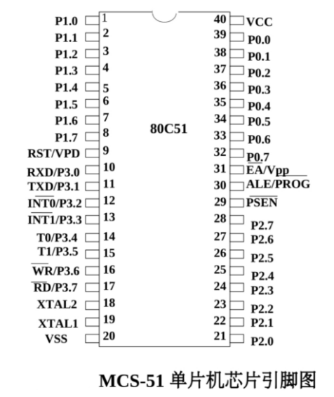
| Microcontroller pins | number | Detailed introduction |
| 4 groups of 8-bit bidirectional parallel I/O ports | x32 | P3 port has a second function |
| Main power pin | x2 | GND、VCC |
| Clock circuit pin | x2 | XTAL1/2 |
| control signal pin | x4 | RST, ALE/PROG not, PSEN not, EA not |
| RST | Reset input terminal. After reset, all registers except SP(07H) and P0~P3(FFH) are set to 0. 单片机运行出错或者进入死循环时,可使其复位后重新运行 单片机的复位有上电自动复位和按钮手动复位两种 |
|
| ALE/PROG非 | 地址锁存允许输入/编程脉冲输入端 | |
| PSEN非 | 片外程序存储器选通控制信号端(只读不写,不需要手动控制) | |
| EA非 | 片内/外程序存储器选择输入端(高电平片内,低电平片外) 注意:片内地址超出4k时,自动执行片外程序存储器的程序; 未超出4k时选择片内,需要手动控制,赋值高电平 |
- CPU的工作原理
| 主要组成部分 | 组成部件 | 关键部件 |
|---|---|---|
| 控制器 | 指令部件、时序部件、操作控制部件 | PC程序计数器(存放和指示下一条要执行的指令的地址寄存器,16位专用寄存器,有自动加1功能) |
| 运算器 | 算数/逻辑部件ALU、暂存器 | ALU由加法器和其他逻辑电路组成,运算结果将通过数据总线送到累加器A,同时影响PSW(程序状态字寄存器)的有关标志位 |
(二)80C51的存储器
- 冯·诺依曼结构:程序存储器和数据存储器统一编址,用同类访问指令
- 哈佛结构(80C51系列单片机):程序存储器和数据存储器在物理结构上是分开的
- 51单片机的存储器:
| 物理上 | 4个存储器 | 片内程序存储器、片外程序存储器、片内数据存储器、片外数据存储器 |
| 逻辑上 | 3个存储器 | 片内外统一编址的程序存储器(64KB) 片内数据存储器(00~FFH) 片外数据存储器(64KB) |

1. 程序存储器
- ROM:片内4KB、片外64KB(以16位的程序计数器PC作为地址指针,故寻址空间是64KB)
- 存放编好的程序和数据表格
- 程序存储器中有特殊用途的存储单元放置跳转指令,用于跳转到用户设计的主程序入口地址或用户安排的中断程序起始地址
| 在程序存储器中,以下7个单元具有特殊用途 | |
|---|---|
| 0000H | 51系列单片机上电复位后,PC=0000H 程序将自动从0000H开始执行指令 |
| 0003H | 外部中断0入口 |
| 000BH | 定时器0溢出中断入口 |
| 0013H | 外部中断1入口 |
| 001BH | 定时器1溢出中断入口 |
| 0023H | 串行口中断入口 |
| 002BH | 定时器2溢出中断入口 (只有AT89S52有) |
2. 数据存储器
- RAM:片内256字节(供用户使用的为低128字节)、片外64KB
- 存放常要改变的中间运算结果、数据暂存或标志位等
- 特殊功能寄存器在地址空间上被划分在数据存储器中,但它们并不作为数据存储器使用
- 片内片外RAM的低地址部分(00~0FFH)的地址码相同,通过不同寻址指令区分。访问片内RAM用“MOV”指令;访问片外RAM用“MOVX”指令
- 片内供用户使用的低128字节(00~7FH)分为三个部分
| 通用工作寄存器区 | 00H~1FH | 4组,每组8个(R0~R7)工作寄存器 由PSW中的RS1、RS0来选择哪一组 不做工作寄存器时,可做通用RAM |
| 位寻址区 | 20H~2FH | 可用位寻址方式访问其每个位 |
| 用户RAM区 | 30H~7FH | 可通过直接或间接寻址方式访问 |
(三)特殊功能寄存器(SFR)
- 用于管理片内和片外的功能部件(定时器、中断系统及外部扩展的存储器、外围芯片等)
- 分布空间:数据存储器的高128位字节地址80F~FFH中
- 51系列的SFR
SFR 名称 位长 具体功能与作用 ACC(A) 累加器A 8 进行算数运算、逻辑类操作
存一个操作数或中间结果
B B寄存器 8 一般寄存器,暂存数据 PSW 程序状态字 8 反映程序运行状态
奇偶标志P、复位标志D1H、溢出标志OV、进位标志CY等
工作寄存器组选择位:RS0、RS1(2位4种状态)
RS1+RS0:00:寄存器第0组:00H~07H
RS1+RS0:01:寄存器第1组:08H~0FH
RS1+RS0:10:寄存器第2组:10H~17H
RS1+RS0:11:寄存器第3组:18H~1FH
P0~P3 端口0~3 8 P0~P3的锁存器 DPTR0/1 数据指针寄存器 16 由两个8位寄存器DPH、DPL组成,用于访问外部数据存储器和程序存储器,寻址范围64K
SP 堆栈指针 8 始终存放着堆栈栈顶的地址
每存入或取出1字节数据,SP就自动加1或减1
始终指向新的栈顶
进栈(PUSH指令):先SP加1,后写入数据
出栈(POP指令):先读出数据,后SP减1
功能:保护现场和保护断点
IP 中断优先级 8 锁存各中断优先级的控制位 IE 中断允许 8 控制中断的开放/关闭 TMOD T0/T1工作方式寄存器
定时器/计数器方式
(不能进行位寻址)
8 M1/M0方式选择位
V/T非 功能选择位
GATE 门空位
(只能用整个字节传送指令设置定时器工作方式)
TCON 中断请求标志
定时器/计数器控制
8 有中断源发出请求时,硬件将相应的中断标志位置1 TH0 定时器/计数器0(高字节) 8 TL0 定时器/计数器0(低字节) 8 TH1 定时器/计数器1(高字节) 8 TL1 定时器/计数器1(低字节) 8 SCON 串行口中断控制
8 SBUF 串行数据缓冲器 8 PCON 电源控制 8 WDTRST 看门狗复位寄存器 8 AUXR1 辅助寄存器 8 
- 区分各种寄存器可参考
简单解释程序计数器、指令寄存器、通用寄存器、状态寄存器、程序状态字![]() https://blog.csdn.net/qq_34246965/article/details/115865306
https://blog.csdn.net/qq_34246965/article/details/115865306
(四)MCS-51产品间区别
- 8051,片内有4K的ROM,本文中所有单片机共性均用8051代表
- 8031,没有ROM,只能扩展ROM才能写程序
- 详细内容可以参考:
详析8031、8051、8751、89C51、89S51的区别与特点![]() https://blog.csdn.net/u011910350/article/details/54600233
https://blog.csdn.net/u011910350/article/details/54600233
三、中断系统
- 详细内容可以参考往期文章(基于C51语言):
中断系统+定时/计数器![]() https://blog.csdn.net/Taylor_Kurt/article/details/125919379
https://blog.csdn.net/Taylor_Kurt/article/details/125919379


四、定时/计数器
- 单片机时钟电路的两种方式:内部自激振荡器并产生振荡时钟脉冲的内部振荡方式;引入外部已有的时钟信号的外部振荡方式
- CPU时序
| 辨析单片机中各类周期(时钟脉冲频率fosc) | ||
| 振荡周期(时钟周期) | 时钟脉冲频率(晶振提供的频率)的倒数 | 1 / fosc |
| 状态周期 | 2个振荡周期 | (1 / fosc) * 2 |
| 机器周期 | 完成一个基本操作所需要的时间 6个状态周期;12个振荡周期 |
(1 / fosc) * 12 |
| 指令周期 | 执行一条指令所需要的时间,由若干个机器周期组成 | n个机器周期 |

- 详细内容可以参考往期文章(基于C51语言):
中断系统+定时/计数器![]() https://blog.csdn.net/Taylor_Kurt/article/details/125919379
https://blog.csdn.net/Taylor_Kurt/article/details/125919379


五、串行通信
- 详细内容可以参考往期文章(基于C51语言):
串行通信![]() https://blog.csdn.net/Taylor_Kurt/article/details/126010269
https://blog.csdn.net/Taylor_Kurt/article/details/126010269
- 串行口的中断,CPU响应中断后,必须在中断服务程序中,用软件清除相应的中断标志位,以撤消中断请求。
- 串行口数据缓冲器SBUF是可以直接寻址的专用寄存器。
- 串行口的中断,CPU响应中断后,必须在中断服务程序中,用软件清除相应的中断标志位,以撤消中断请求。
- 串行口数据缓冲器SBUF在物理上是2个8位寄存器,共用地址99H;
- 读SBUF发送(MOV SBUF,A)
- 写SBUF接收(MOV A,SBUF)


·构成单片机的最小系统:单片机、时钟电路、复位电路
·单片机应用系统:在单片机系统的基础上配置了面向对象的接口电路。前向通道,有A/D、开关量输入等;后向通道,有D/A、开关量输出等;人机交互通道,有键盘、显示、打印机等;串行通信接口,有RS232C、RS422/485、CAN总线等。
·须外界上拉电阻的I/O口:P0口,作一般I/O口时输出为漏极开路,须外接上拉电阻(内部没有上拉电阻)
·读引脚须执行两条指令:
MOV P1,#0FFH ;P1=0XFF关闭场效应管,置P1为输入口
MOV A,P1 ;A=P1
·A/D转换须执行两条指令:
MOV DPTR,#0FEF8H ;指向扩展芯片的首地址
MOVX @DPTR,A ;启动A/D转换
·中断响应后,CPU完成以下自主操作:
(1)中断标志自动清“0”(RI/TI除外)
(2)断点地址压入堆栈保护
(3)中断入口地址装入PC,使程序转向中断入口地址单元中去执行相应的中断服务程序
·中断返回,执行RETI指令,产生以下自主操作:断点地址弹给PC,以便程序返回断点处继续执行
·定时器初始化(4步):
(1)TMOD,确定工作方式
(2)THi、TLi,装入计数初值
(3)置TRi=1,启动Ti
(4)置ETi=1,开Ti中断;置EA=1,开CPU总中断,
·定时器初值(X)计算:X = M - 计数值 (M为最大计数值,方式1 = 65536,方式2 = 256)
例如:时钟频率为6MHz,产生1ms的定时,计算初值
机器周期 ( 1 / 6MHz )* 12 = 2μs
计数值 1ms = 1000μs = 2μs * 500次 则计数值为500
计数初值(方式1) X = 65536 - 500 = 65036
计数初值(方式2) X = 256 - 500 = 156
·定时器赋初值十进制——>十六进制
除以16取余数得最低位,然后把商继续除以16得次低位,直到商等于0
65036 除以 16,余数 12(C),商4064
4064 除以 16,余数 0(0),商254
254 除以 16,余数 14(E),商15
15除以16,余数 15(F),商0,结束
得十进制的65036转化成十六进制为 FE0C
·通信的基本方式:
并行通信:所传输数据的各位同时发送或接收
串行通信:所传输数据的各位按顺序一位一位地发送或接收
·串行通信工作方式:
(从传输方式)单工方式、半双工方式、全双工方式
(从接收方式)同步通信、异步通信
·串行通信波特率:
数据传送速率,表示每秒钟传送多少位二进制数,常用于多机通信

·注意:在51单片机中需要使用定时器1来产生波特率,因此,如果使用串口通信,则定时器1就不能做其他用途,在初始化串口时,除了配置SCON寄存器,还要根据波特率参数设置定时器1的计数初值;定时器T1作波特率发生器时,应选用工作方式2(8位自动重载方式),可避免通过程序反复装入初值引起的定时误差,使波特率更加稳定。发送数据时,低位在前,高位在后
·多机通信流程(判断多机通信控制位SM2和发送或接收的第9数据位【D8】)
(1)串行口以方式2或3接收,所有从机初始化将多机通信位SM2置1,允许多机通信
(2)主机将发送数据第九位TB8置1,发送要寻址的从机地址
(3)所有从机均接收到主机发送的地址,并进行地址比较
(4)从机符合,则将SM2置0,向主机返回地址,供主机核对;若不符合,SM2仍保持1
(5)核对无误后,主机向被寻址从机发送命令,通知从机接收或发送数据
(6)通讯结束后,本、从机置SM2为1
·串口初始化:
(1)设置波特率
①TMOD,确定定时器1的工作方式
②TH1、TL1,设置定时器1的初值
③TR1 启动定时器1
(2)SCON,确定串口的控制
(3)开ES、EA