Table of contents
- 1 Introduction
- 2. The GT high-speed interface solution I have here
- 3. The most detailed interpretation of GTX network
- 4. Design thinking framework
- 5. Detailed explanation of the first set of vivado projects
- 6. Detailed explanation of the second group of vivado projects
- 7. Board debugging and verification
- 8. Benefits: Acquisition of engineering codes
1 Introduction
I am ashamed to say that I have played FPGA before if I have never played GT resources. This is a sentence said by a big guy at CSDN, and I firmly believe it. . .
GT resources are an important selling point of Xilinx series FPGAs, and they are also the basis for high-speed interfaces. Whether it is PCIE, SATA, MAC, etc., GT resources are required for high-speed serialization and deserialization of data. Different FPGA series of Xilinx have different GT resource type, the low-end A7 has GTP, K7 has GTX, V7 has GTH, and the higher-end U+ series has GTY, etc. Their speed is getting higher and higher, and their application scenarios are becoming more and more high-end. . .
This article uses the GTX resources of Xilinx's Kintex7 FPGA to do board-to-board video transmission experiments. There are two video sources, corresponding to whether the developer has a camera or not. One is to use a cheap OV5640 camera module; if you succeed If there is no camera in your computer, or your development board has no camera interface, you can use the dynamic color bars generated inside the code to simulate the camera video; the video source is selected through the `define macro definition at the top of the code, and ov5640 is used as the video source by default, calling GTX IP core, use verilog to write codec module and data alignment module of video data, use 2 SFP optical ports on 2 development board hardware to realize data transmission and reception; this blog provides 2 sets of vivado project source code, the difference between 2 sets of projects One set is for GTX transmission, and the other is for GTX reception; this blog describes the design scheme of FPGA GTX video transmission in detail, the engineering code can be comprehensively compiled and debugged on the board, and can be directly transplanted. It is suitable for school students and postgraduate project development , is also suitable for on-the-job engineers to do learning improvement, and can be applied to high-speed interfaces or image processing fields in medical, military and other industries; provide
complete and smooth engineering source code and technical support; the
acquisition method of engineering source code and technical support is placed in At the end of the article, please be patient to see the end;
disclaimer
This project and its source code are partly written by myself, and partly obtained from public channels on the Internet (including CSDN, Xilinx official website, Altera official website, etc.). The project and its source code are limited to the personal study and research of readers or fans, and commercial use is prohibited. If the legal issues caused by the commercial use of readers or fans for their own reasons have nothing to do with this blog and the blogger, please use it with caution. . .
2. The GT high-speed interface solution I have here
My homepage has a FPGA GT high-speed interface column, which includes video transmission routines and PCIE transmission routines for GT resources such as GTP, GTX, GTH, and GTY, among which GTP is based on A7 series FPGA development boards, and GTX is based on K7 or ZYNQ series FPGA development board is built, GTH is built based on KU or V7 series FPGA development board, GTY is built based on KU+ series FPGA development board; the following is the column address:
click to go directly
3. The most detailed interpretation of GTX network
The most detailed introduction to GTX must be Xilinx's official "ug476_7Series_Transceivers", we use this to interpret:
I have put the PDF document of "ug476_7Series_Transceivers" in the data package, and there is a way to obtain it at the end of the article; the
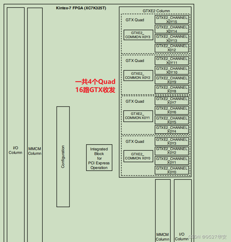
FPGA model of the development board I used It is Xilinx Kintex7 xc7k325tffg676-2; it has 8 channels of GTX resources, 2 of which are connected to 2 SFP optical ports, and the sending and receiving speed of each channel is between 500 Mb/s and 10.3125 Gb/s. GTX transceivers support different serial transmission interfaces or protocols, such as PCIE 1.1/2.0 interface, 10 Gigabit network XUAI interface, OC-48, serial RapidIO interface, SATA (Serial ATA) interface, digital component serial interface (SDI) etc;
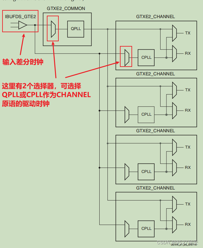
GTX basic structure
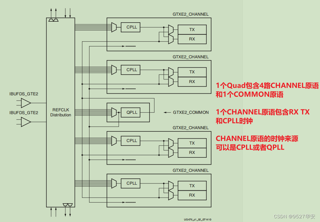
Xilinx uses Quad to group serial high-speed transceivers. Four serial high-speed transceivers and a COMMOM (QPLL) form a Quad. Each serial high-speed transceiver is called a Channel (channel). The figure below shows four The schematic diagram of the GTX transceiver in the Kintex7 FPGA chip: "ug476_7Series_Transceivers" page 24; the
specific internal logic block diagram of GTX is shown below, which consists of four transceiver channels GTXE2_CHANNEL primitives and a GTXE2_COMMON primitive. Each GTXE2_CHANNEL includes a transmitting circuit TX and a receiving circuit RX. The clock of GTXE2_CHANNEL can come from CPLL or QPLL, which can be configured in the IP configuration interface; "ug476_7Series_Transceivers" page 25;
The logic circuit of each GTXE2_CHANNEL is shown in the figure below: "ug476_7Series_Transceivers" page 26;
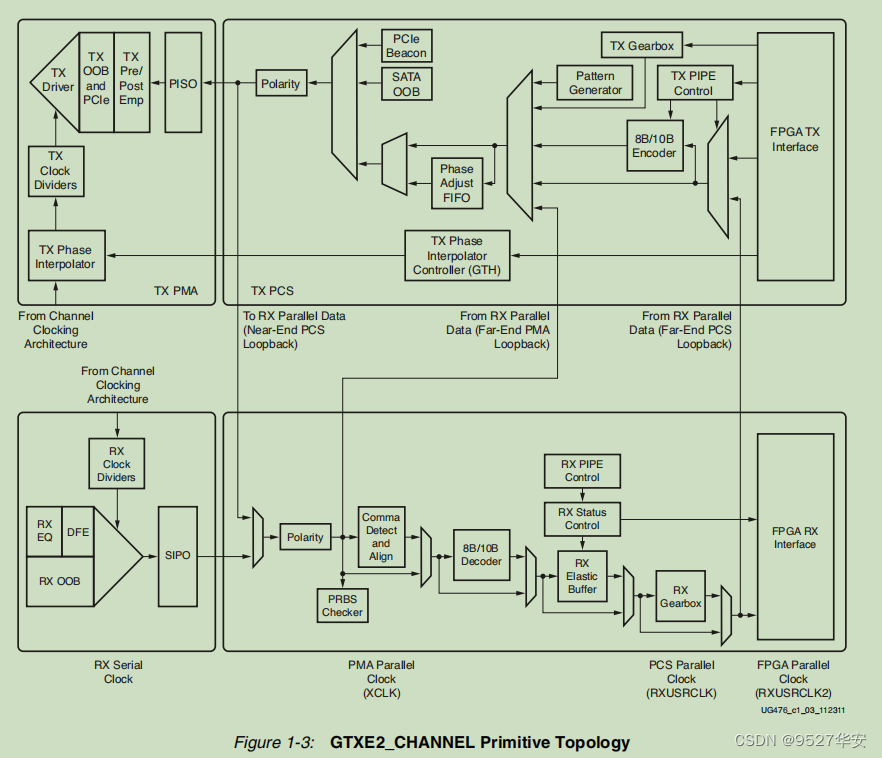
the function of the sending end and receiving end of GTXE2_CHANNEL is independent, and both are composed of PMA (Physical Media Attachment, physical media adaptation layer) and PCS (Physical Coding Sublayer , physical coding sublayer) consists of two sublayers. The PMA sublayer includes high-speed serial-to-parallel conversion (Serdes), pre-/post-emphasis, receiving equalization, clock generator and clock recovery circuits. The PCS sublayer includes circuits such as 8B/10B codec, buffer, channel bonding, and clock correction.
It doesn’t make much sense to say too much here, because if you haven’t done a few big projects, you won’t understand what’s inside. For first-time users or fast users, more energy should be focused on the calling and use of IP cores , I will also focus on the call and use of the IP core later;
GTX send and receive processing flow
First, the user logic data enters a sending buffer (Phase Adjust FIFO) after being encoded by 8B/10B. This buffer is mainly used for clock isolation between the two clock domains of the PMA sublayer and the PCS sublayer, and solves the clock rate matching and phase adjustment between the two. For the problem of difference, the parallel-to-serial conversion (PISO) is performed through high-speed Serdes. If necessary, pre-emphasis (TX Pre-emphasis) and post-emphasis can be performed. It is worth mentioning that if you accidentally cross-connect the TXP and TXN differential pins during PCB design, you can make up for this design error through polarity control (Polarity). The receiving end and the sending end process are opposite, and there are many similarities, so I won’t go into details here. It should be noted that the elastic buffer of the RX receiving end has clock correction and channel binding functions. Every function point here can write a paper or even a book, so here you only need to know a concept, and you can use it in a specific project, or the same sentence: For the first time or want to use it quickly For those who are concerned, more energy should be focused on the calling and use of IP cores.
Reference clock for GTX
The GTX module has two differential reference clock input pins (MGTREFCLK0P/N and MGTREFCLK1P/N), which can be selected by the user as the reference clock source of the GTX module. On the general A7 series development board, there is a 148.5Mhz GTX reference clock connected to MGTREFCLK0 as the reference clock of GTX. The differential reference clock is converted into a single-ended clock signal by the IBUFDS module and entered into the QPLL or CPLL of GTXE2_COMMOM to generate the required clock frequency in the TX and RX circuits. If the TX and RX transceiver speeds are the same, the TX circuit and the RX circuit can use the clock generated by the same PLL. If the TX and RX transceiver speeds are not the same, the clocks generated by different PLL clocks need to be used. Reference clock Here, the GT reference routine given by Xilinx has been done very well, and we don’t need to modify it when we call it; the reference clock structure diagram of GTX is as follows: "ug476_7Series_Transceivers" page 31;
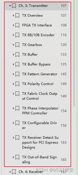
GTX transmit interface
Pages 107 to 165 of "ug476_7Series_Transceivers" introduce the sending process in detail, and most of the content can be ignored by users, because the manual basically talks about his own design ideas, leaving the user's operable interface and Not many, based on this idea, we focus on the interface that needs to be used in the sending part left to the user when instantiating GTX;
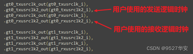
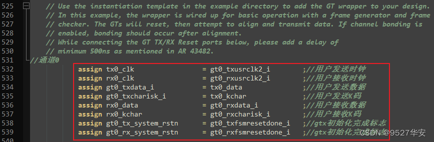
Users only need to care about the clock and data of the sending interface. This part of the interface of the GTX instantiation module is as follows:
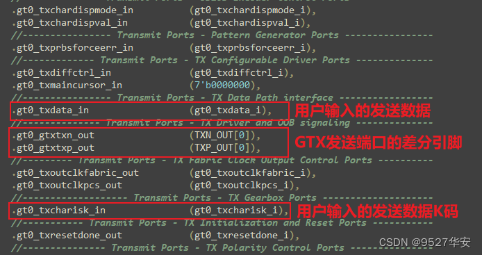
In the code, I have re-bound and made the top layer of the module for you. The code part is as follows:
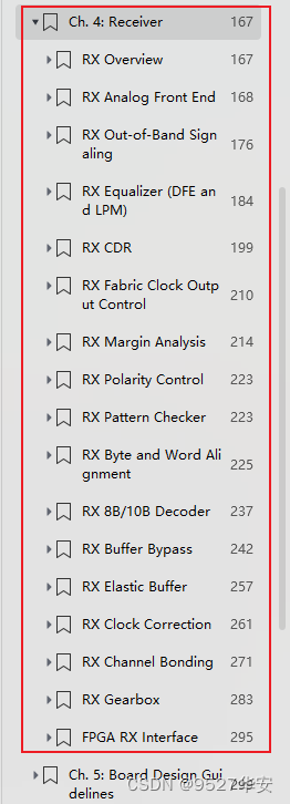
GTX receiving interface
Pages 167 to 295 of "ug476_7Series_Transceivers" introduce the transmission process in detail, and most of the content can be ignored by users, because the manual basically talks about his own design ideas, leaving the user's operable interface and Not many, based on this idea, we will focus on the interfaces that the user needs to use in the sending part of the GTX instantiation; the
user only needs to care about the clock and data of the receiving interface. The interface of this part of the GTX instantiation module is as follows:
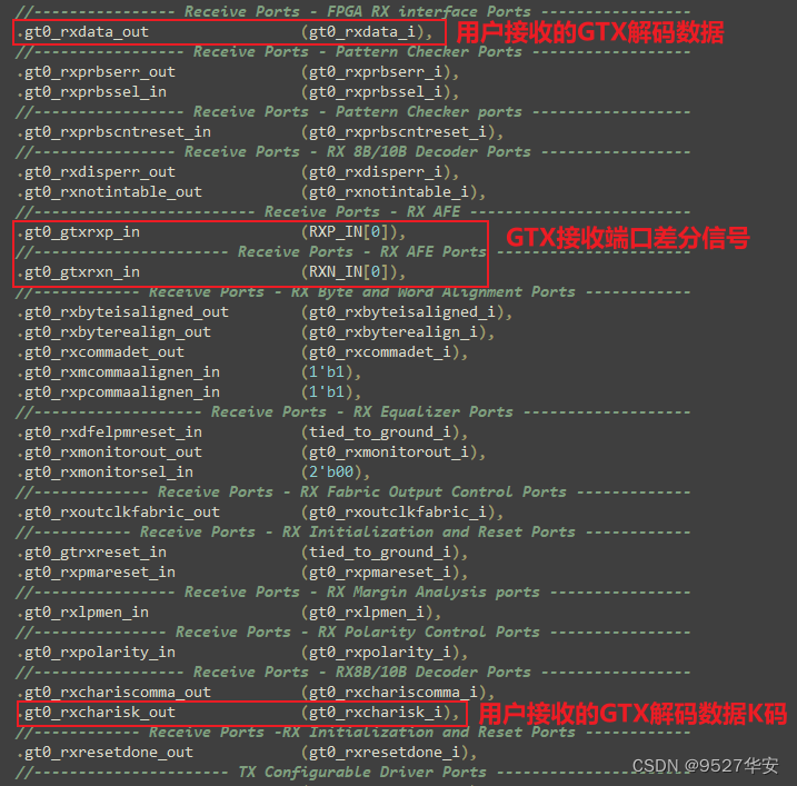
In the code, I have rebinded for you and made it to the top level of the module, the code part is as follows:
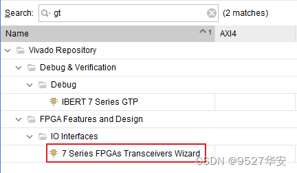
Call and use of GTX IP core
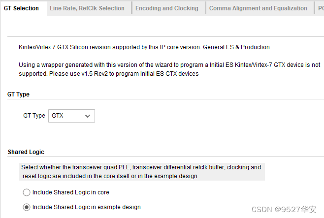
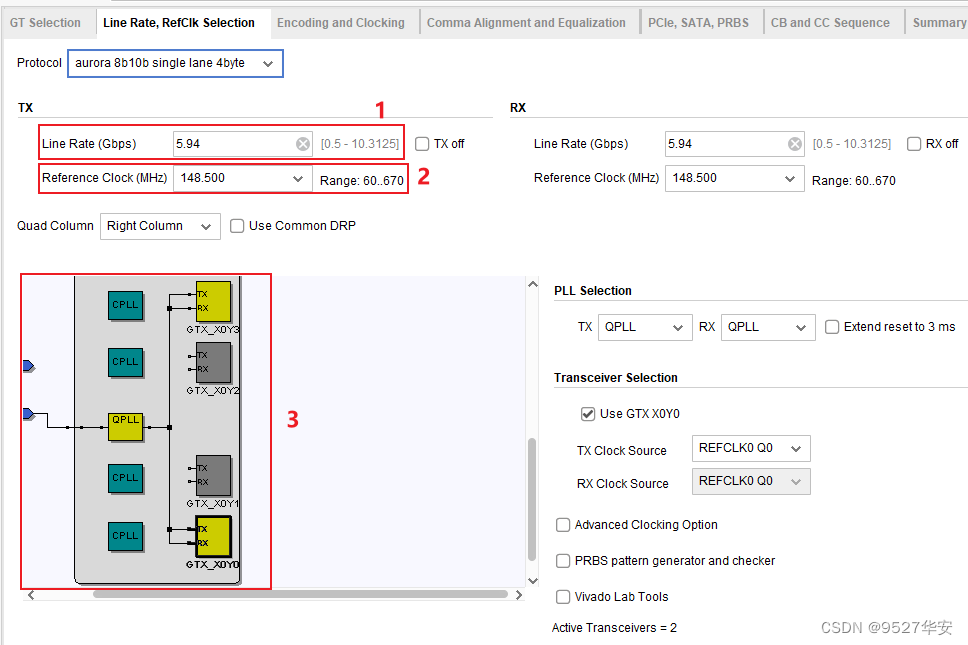
Here is an explanation of the labels in the above picture:
1: Line rate. According to your own project requirements, the range of GTX is 0.5 to 10.3125G. Since my project is video transmission, it can be within the range of GTX rate. In this example 2: Reference
clock, this depends on your schematic diagram, it can be 80M, 125M, 148.5M, 156.25M, etc. My development board is 148.5M; 4:
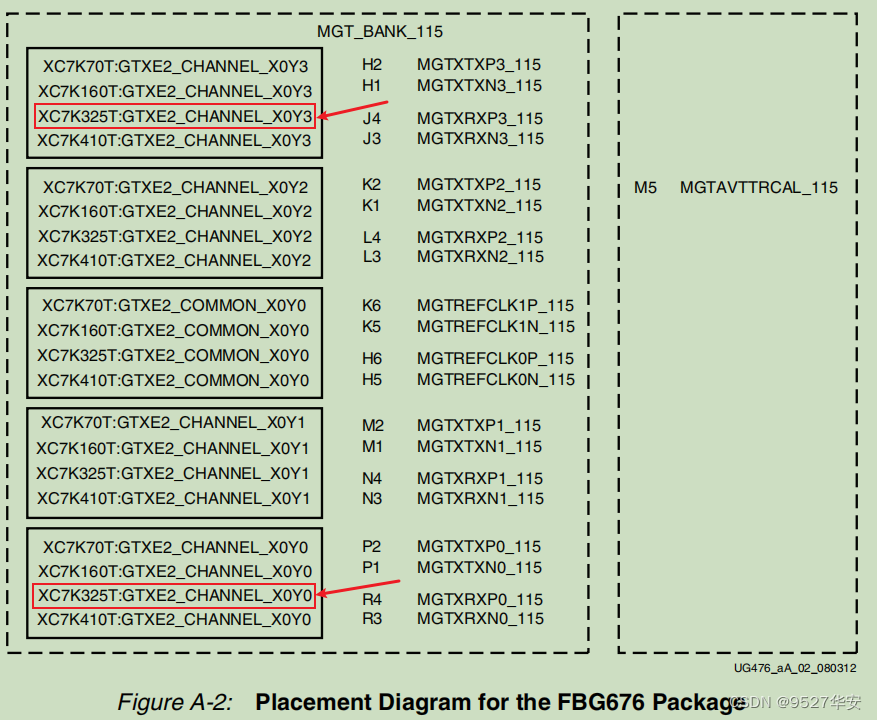
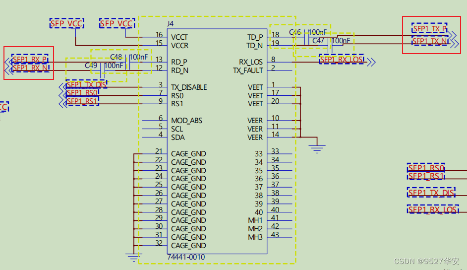
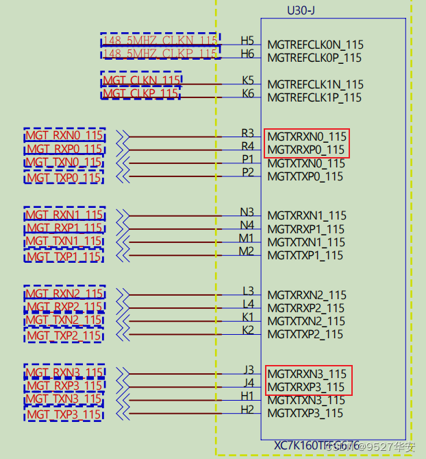
GTX group binding, This is very important. There are two references for his binding. It is your development board schematic diagram, but the official reference "ug476_7Series_Transceivers". The official GTX resources are divided into multiple groups according to different banks, because the GT resources are Xilinx The dedicated resources of the series FPGA occupy a dedicated Bnak, so the pins are also dedicated, so how do these GTX groups and pins correspond? The description of "ug476_7Series_Transceivers" is as follows: the red box is the FPGA pin corresponding to the schematic diagram of my development board; the
schematic diagram of my board is as follows:
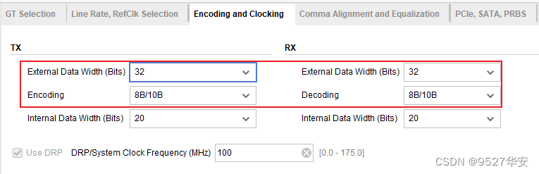
Select the 8b/10b codec with an external data bit width of 32 bits, as follows: The
following is about K code detection: here
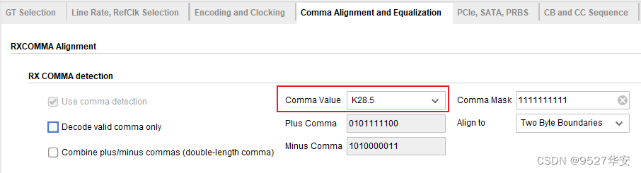
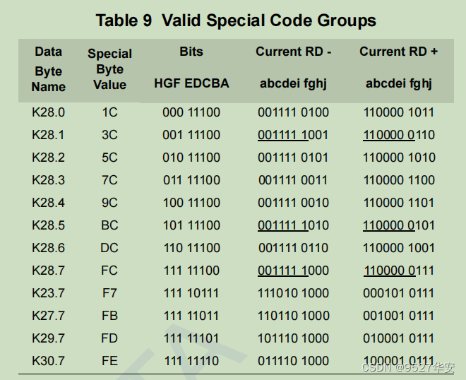
choose K28.5, which is the so-called COM code, and the hexadecimal system is bc. It has many functions and can be Indicates an idle out-of-sequence symbol, and can also indicate a data misalignment flag, which is used to indicate data misalignment here. The 8b/10b protocol defines the K code as follows: The following is about clock correction, which is the elastic buffer corresponding to the internal receiving part of GTP
;
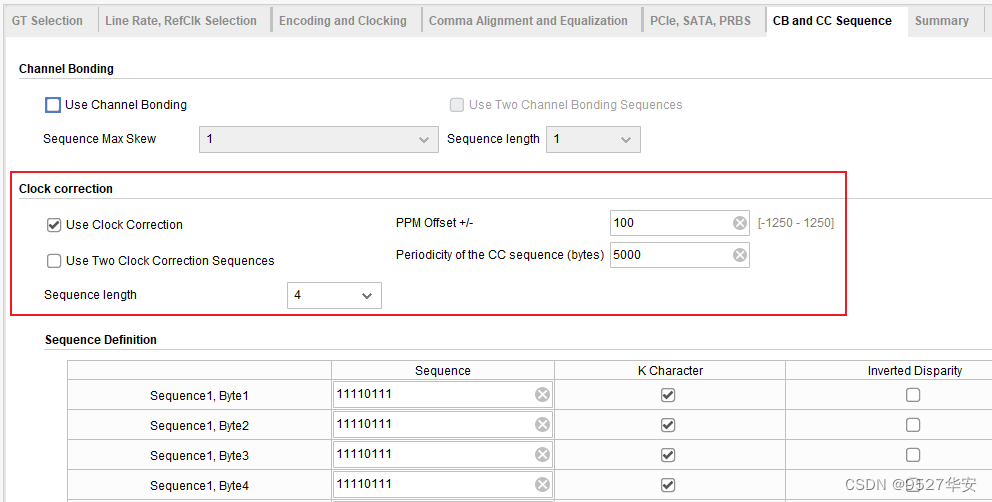
here There is a concept of clock frequency offset, especially when the clocks of the sending and receiving parties are from different sources, the frequency offset set here is 100ppm, and it is stipulated that the sender sends a 4-byte sequence every 5000 data packets, and the elastic buffer of the receiver will be based on this The 4-byte sequence and the position of the data in the buffer determine whether to delete or insert a byte in a 4-byte sequence, in order to ensure the stability of the data from the sender to the receiver and eliminate the influence of clock frequency offset;
4. Design thinking framework
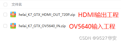
This blog provides 2 sets of vivado project source code. The difference between the 2 sets of projects is that one set is sent by GTX, and the other set is received by GTX; I have two FPGA development boards here, which are recorded as development board 1 and development board 2. There are OV5640 input and HDMI output interfaces on the development board. The source codes of two sets of vivado projects are as follows and the design structure is as follows:
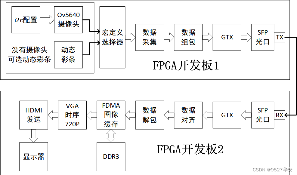
The first set of vivado project source codes: GTX is used as the sender, FPGA development board 1 collects video, and then the data is packaged and processed by GTX. After 8b/10b encoding, it is sent out through the TX end of the onboard SFP optical port; there are two video sources, corresponding to whether the developer has a camera or not, one is to use a cheap OV5640 camera module; if you If you don’t have a camera, or your development board doesn’t have a camera interface, you can use the dynamic color bars generated inside the code to simulate the camera video; the video source is selected through the `define macro definition at the top level of the code, and ov5640 is used as the video source by default;
The second set of vivado project source code: the SFP RX port of the FPGA2 development board receives data, and after GTX performs 8b/10b decoding, data alignment, and data unpacking operations, effective video data is obtained, and then I use my usual FDMA scheme to make Video cache, finally output HDMI video display;
Video source selection
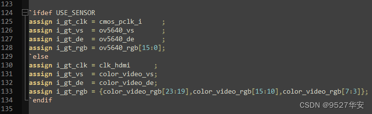
There are two types of video sources, corresponding to whether the developer has a camera or not. If you have a camera in your hand, or if your development board has a camera interface, use the camera as the video input source. What I use here is a cheap The OV5640 camera module; if you don’t have a camera in your hand, or your development board has no camera interface, you can use the dynamic color bars generated inside the code to simulate camera video. The dynamic color bars are moving pictures, which can completely simulate video; default Use ov5640 as the video source; the selection of the video source is carried out through the `define macro definition at the top of the
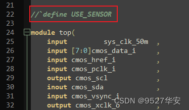
code ; No comment) When define USE_SENSOR, the input source video is ov5640 camera;
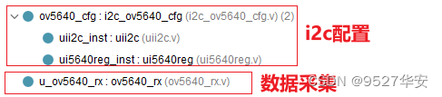
OV5640 camera configuration and acquisition
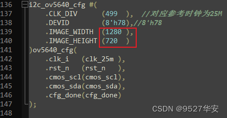
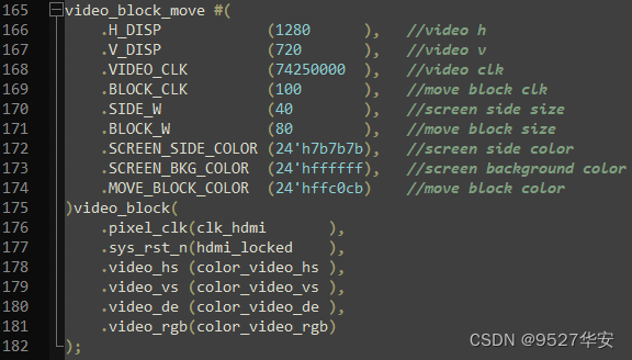
The OV5640 camera requires i2c configuration before it can be used. It is necessary to collect the video data of the DVP interface as video data in RGB565 or RGB888 format. Both parts are implemented with verilog code modules. The code location is as follows: The camera is configured with a resolution of 1280x720, as follows
:
Camera The acquisition module supports video output in RGB565 and RGB888 formats, which can be configured by parameters, as follows:
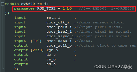
RGB_TYPE=0 outputs the original RGB565 format;
RGB_TYPE=1 outputs the original RGB888 format;
the design selects the RGB565 format;
dynamic color bar
The dynamic color bar can be configured as videos with different resolutions. The border width of the video, the size of the dynamic moving square, and the moving speed can all be parameterized. I configure the resolution here as 1280x720, the code position of the dynamic color bar module and the top-level interface and Instantiated as follows:

video packet
Since the video needs to be sent and received through the aurora 8b/10b protocol in GTP, the data must be packaged to adapt to the aurora 8b/10b protocol standard; the code position of the video data package module is as follows: first, we store the 16bit video in the
FIFO , when a line is full, it is read from the FIFO and sent to GTX for transmission; before that, a frame of video needs to be numbered, which is also called an instruction. When GTX packs, it sends data according to a fixed instruction. The command restores the video field synchronization signal and video effective signal; when the rising edge of a frame of video field synchronization signal arrives, send a frame of video start instruction 0, and when the falling edge of a frame of video field synchronization signal arrives, send a frame Video start command 1, send invalid data 0 and invalid data 1 during the video blanking period, number each line of video when the video valid signal arrives, first send a line of video start command, and then send the current video line number, when a line of video is sent After completion, send a line of video end command. After sending a frame of video, first send a frame of video end command 0, and then send a frame of video end command 1; so far, a frame of video is sent. This module is not easy to understand. So I made detailed Chinese comments in the code. It should be noted that in order to prevent the disordered display of Chinese comments, please open the code with notepad++ editor; the command definition is as follows: the command can be changed arbitrarily, but the lowest byte must be
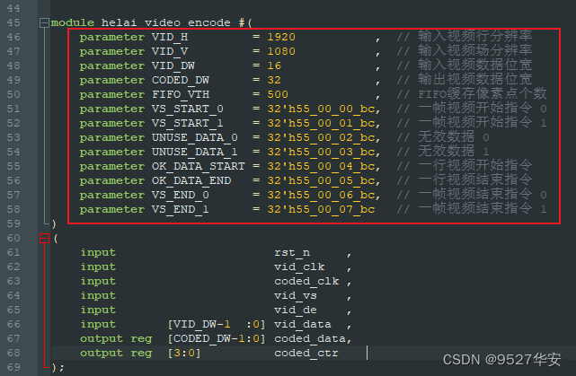
bc ;
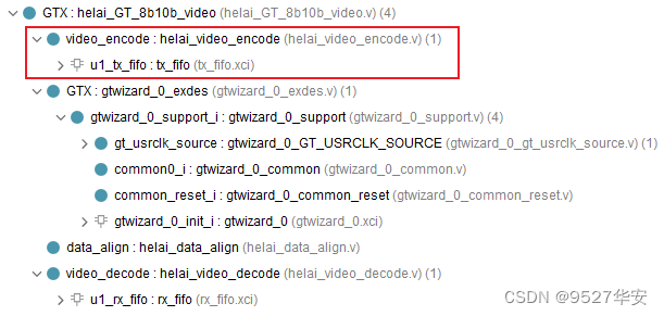
GTX aurora 8b/10b
This is to call GTX to do the data encoding and decoding of the aurora 8b/10b protocol. I have already made a detailed overview of GTX before, so I won’t talk about it here; the code location is as follows:
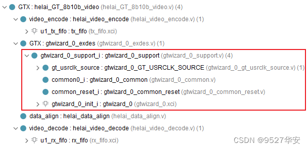
data alignment
Since the aurora 8b/10b data transmission and reception of GT resources naturally has data misalignment, it is necessary to perform data alignment processing on the received decoded data. The code position of the data alignment module is as follows: The K code control character format I defined is: XX_XX_XX_BC, so
use One rx_ctrl indicates whether the data is a K-code COM symbol;
rx_ctrl = 4'b0000 indicates that the 4-byte data has no COM code;
rx_ctrl = 4'b0001 indicates that [7: 0] in the 4-byte data is a COM code;
rx_ctrl = 4'b0010 means [15: 8] in the 4-byte data is the COM code;
rx_ctrl = 4'b0100 means the [23:16] in the 4-byte data is the COM code;
rx_ctrl = 4'b1000 means the 4-byte [31:24] in the data is the COM code;
based on this, when the K code is received, the data will be aligned, that is, the data will be patted and combined with the new incoming data. This is the basis of FPGA Operation, no more details here;
Video data unpacking
Data unpacking is the reverse process of data packet packaging, and the code position is as follows:
When GTX unpacks, it restores the video field synchronization signal and video effective signal according to fixed instructions; these signals are important signals for the subsequent image cache;
so far, the data enters and exits GTX The part has been finished, and the block diagram of the whole process is described in the code, as follows:
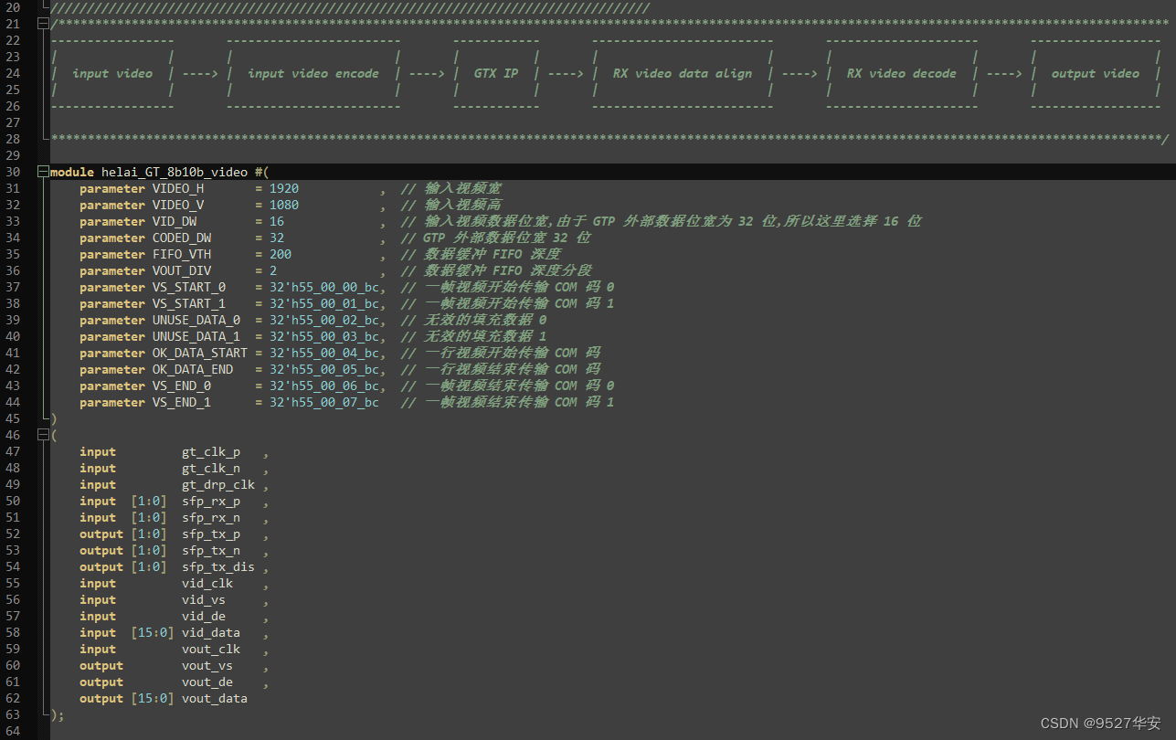
image cache
Old fans who often read my blog should know that my routine for image caching is FDMA. Its function is to send images to DDR for 3 frame buffers and then read them out for display. The purpose is to match the clock difference between input and output and improve output. Video quality, about FDMA, please refer to my previous blog, blog address: click to go directly
video output
After the video is read from FDMA, it will be output to the display after passing through the VGA timing module and the HDMI sending module. The code position is as follows: The VGA timing
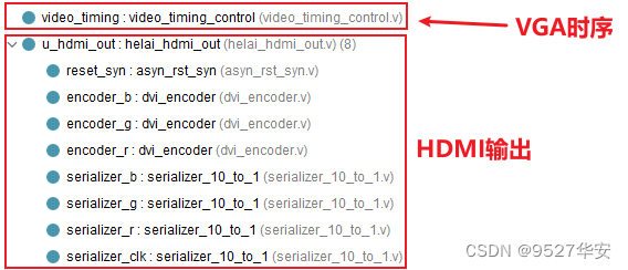
configuration is 1280X720, and the HDMI sending module is handwritten with verilog code, which can be used for FPGA HDMI sending applications. About this module, Please refer to my previous blog, blog address: click to go directly
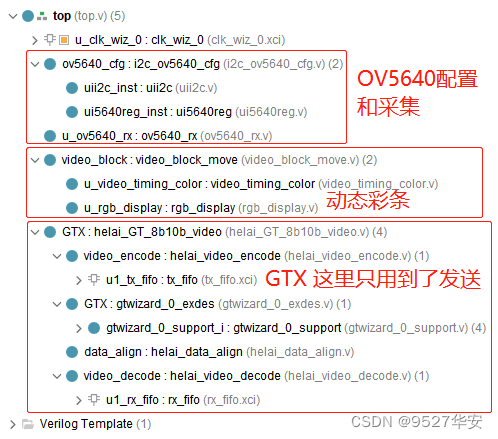
5. Detailed explanation of the first set of vivado projects
Development board FPGA model: Xilinx–Kintex7–xc7k325tffg676-2;
development environment: Vivado2019.1;
input: ov5640 camera or dynamic color bar, resolution 1280x720@60Hz;
output: TX interface of the SFP optical port of development board 1;
application: GTX board-to-board video transmission;
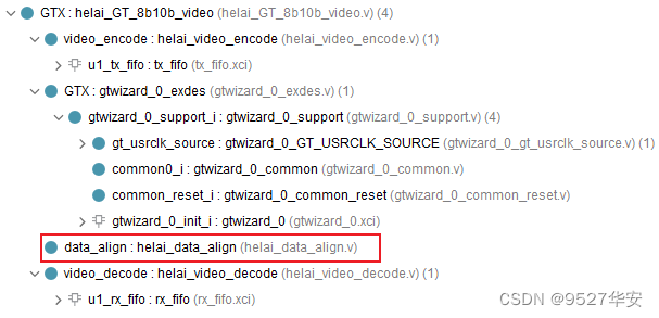
the engineering code structure is as follows:
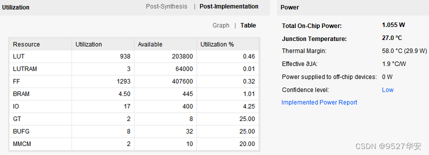
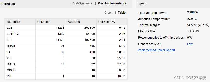
FPGA resource consumption and power consumption estimation after comprehensive compilation is as follows:
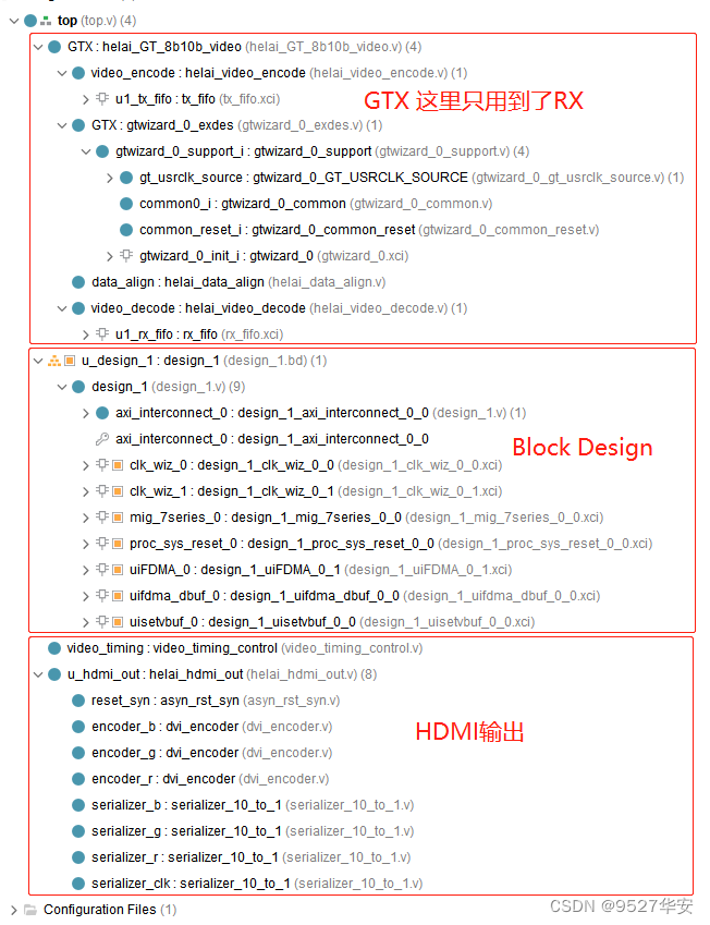
6. Detailed explanation of the second group of vivado projects
Development board FPGA model: Xilinx–Kintex7–xc7k325tffg676-2;
development environment: Vivado2019.1;
input: RX interface of the SFP optical port of development board 2;
output: HDMI output interface of development board 2, with a resolution of 1280X720@60Hz;
Application: GTX board-to-board video transmission;
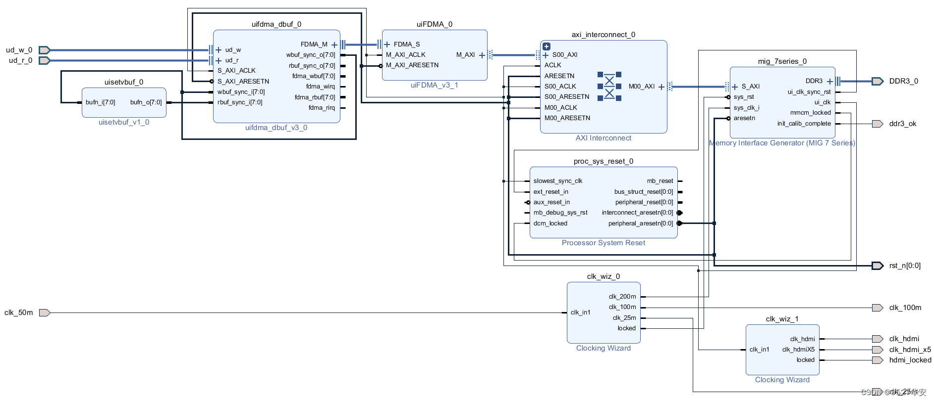
the project Block Design is as follows:
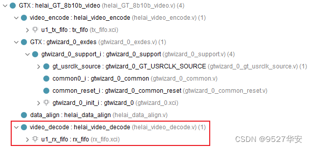
the project code structure is as follows:
FPGA resource consumption and power consumption estimation after comprehensive compilation is as follows:
7. Board debugging and verification
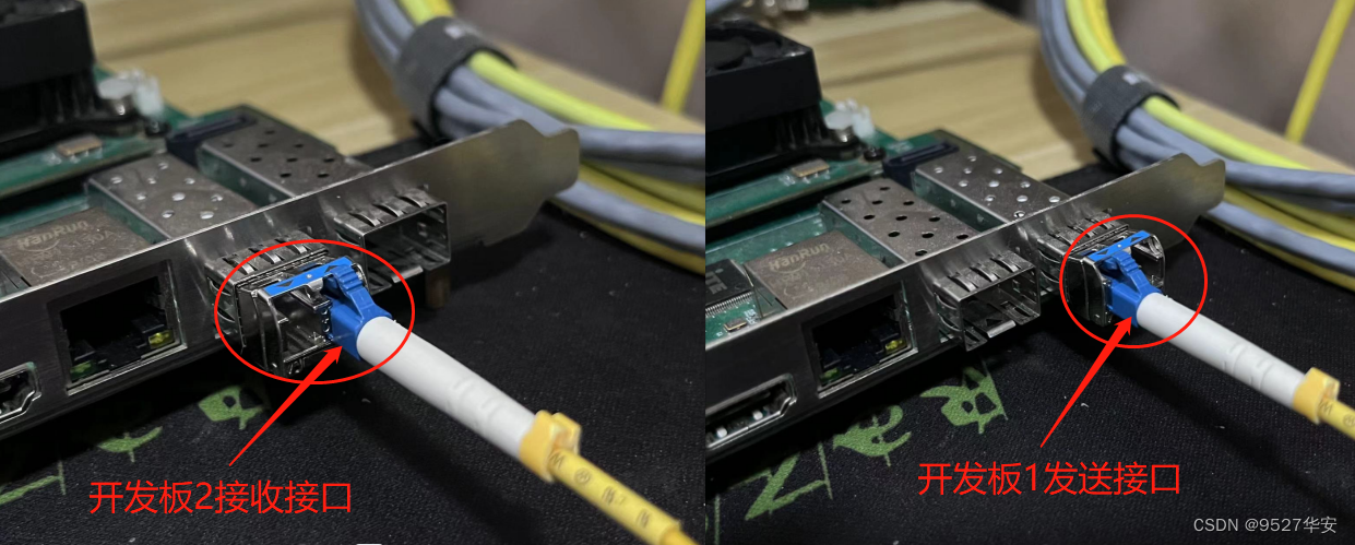
fiber optic connection
The optical fiber connections of the two boards are as follows:
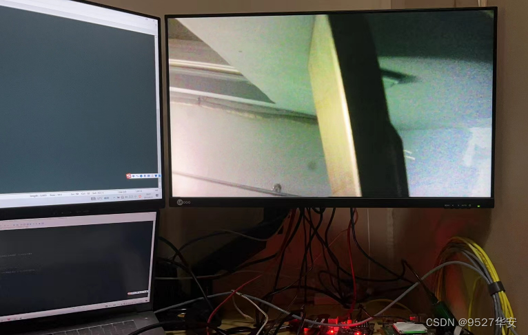
static demo
The following takes the two boards of the first group of vivado projects as an example to show the output effect:
when the GTX runs at a 4G line rate, the output is as follows:
8. Benefits: Acquisition of engineering codes
Benefits: Obtaining the engineering code
The code is too large to be sent by email, and it is sent by a certain degree network disk link. The
method of data acquisition: private, or the V business card at the end of the article.
The network disk information is as follows: