Article directory
Starting from this article, I will take the Renesas RA series wildfire_Qiming 6M5 development board (R7FA6M5BH3CFC) as an example to share the fun of learning with you
1. Introduction to IOPORT
Chip pins can be roughly divided into IO pins and non-IO pins. Non-IO pins are those pins such as power supply pins, crystal oscillator pins, etc., and they do not have GPIO (general-purpose input and output) functions. The IO pins are those with GPIO functions, they can be configured in various modes and implement various general functions.
The most basic output function of the IO pin is to output high and low levels to realize switch control (such as switching LED lights, relays or triodes, etc.); the most basic input function is to detect external input levels (such as through pin level high and low to distinguish whether the button is pressed). IO pins can also be used to connect external devices, communicate with external devices, send control commands, collect sensor data, and so on.
IOPORT is I/O Port, which is written as "IOPORT" in the code for convenience, indicating input and output ports. IOPORT is a peripheral module of RA MCU, which is used to control the pins of the chip and configure each pin in detail. Specifically, IOPORT can configure the pins in the following aspects:
-
Configure the pin as a common IO function, that is, input or output high level or low level.
-
Input pull-up resistor for CONTROL pin.
-
Controls the drive capability of the pin.
-
Controls whether the pin detects rising/falling/both edges.
-
Whether the control pin is used as an interrupt input pin.
-
Configure the pin as an analog input function or connect the pin internally to other peripheral modules.
The IO ports of Renesas RA series chips are theoretically divided into 16 groups (0~9, A, B, C, D, E, F), each group has 16 pins (0~15). However, the actual situation is not a complete "16 groups + 16 pins per group" configuration, but varies with the actual chip model. Take the R7FA6M5BH3CFC chip on the Wildfire Qiming 6M5 board as an example. It is a LQFP 176-pin package with a total of 176 pins, most of which are IO pins that can be controlled by the IOPORT module. And these IO pins are divided into 11 groups of pins 0~9, A, B (Note: A, B is the hexadecimal representation of 10, 11), each group generally has 16 pins (pin number 0~15), in fact some groups have less than 16 pins. For packages with fewer pins (LQFP 144-pin and LQFP 100-pin packages), the number of available IO pins of the chip will also be relatively reduced.
2. Block diagram analysis of IOPORT
The block diagram structures of the IOPORT modules of RA6M5, RA4M2, and RA2L1 are basically the same.
Taking RA6M5 as an example, the figure below is the functional structure block diagram of the peripheral IOPORT of RA6M5, and the place marked with the letter A indicates the actual IO pin of the chip.
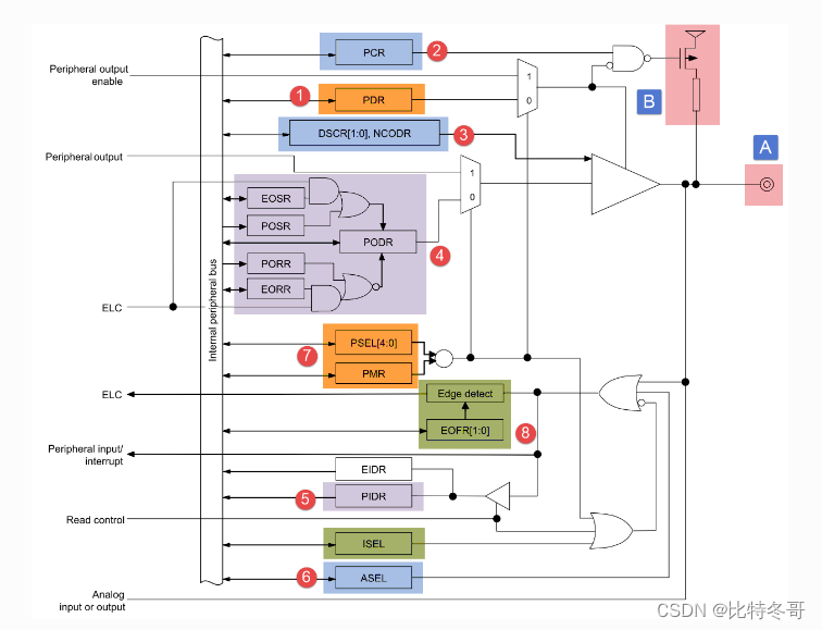
Next, we analyze the structural block diagram of IOPORT peripherals, and it is not difficult to conclude that IOPORT has the following working modes:
-
General-purpose input and output (GPIO) mode
Input mode (floating/pull-up)
output mode (push-pull/open-drain) -
Analog input function mode
-
multiple function mode
1. IO port direction
See mark ① in the figure.
PDR (Port Direction Register) is the port direction register, which controls the GPIO direction of the port. When the IO pin needs to control output high level or low level, the GPIO direction of the pin can be set as GPIO output; and when the level of the IO pin needs to be read, the GPIO direction of the pin can be set as GPIO input.
2. IO input pull-up control
See mark ② in the figure.
PCR (Pull-up Control Register) is a pull-up control register, which controls whether the GPIO input of the IO pin is enabled for pull-up. When it is set to allow pull-up, it will actually connect the weak pull-up resistor at the letter B in the figure to the positive pole of the VCC power supply, thus making the pin in weak pull-up input mode. It should be noted that the weak pull-up resistor can only be used when the GPIO direction of the pin is configured as "input". It can also be seen from the above figure that the IO port of RA6M5 has no pull-down resistor.
3. IO drive capability and open-drain output control
See mark ③ in the figure.
DSCR (Port Drive Capability Register) is a port drive capability register, which controls the drive capability of IO pins. The drive capability refers to the current intensity driven by the IO and the maximum toggle rate of the IO.
NCODR (N-Channel Open-Drain Control Register) is an open-drain output control register, which controls whether the IO pin enables open-drain mode. When the GPIO direction of the pin is configured as "output", the output mode of the IO pin can be configured as push-pull output or open-drain output.
4. IO port output data
See mark ④ in the figure.
This part seems complicated, but in fact, the arrows of EOSR, POSR, PORR, and EORR all point to PODR in the end, which means that the operation of registers such as EOSR, POSR, PORR, and EORR will actually operate on the PODR register.
-
In the figure, PODR (Port Output Data Register) is the port output data register, which controls the output level of the GPIO pin. When the GPIO direction of the pin is configured as "output", the pin can be configured to output high level or low level.
-
In the figure, EOSR (Event Output Set Register) is the event output set register (we ignore this register for now).
-
In the figure, POSR (Pmn Output Set Register) is the port output data register, which controls the output of the GPIO pin to be high level, but cannot control the output low level.
-
In the figure, PORR (Pmn Output Reset Register) is the port output data register, which controls the output of the GPIO pin to be low level, but cannot control the output high level.
-
In the figure, EORR (Event Output Reset Register) is the event output reset register (we ignore this register for now).
5. IO port input data
See mark ⑤ in the figure.
PIDR (Port Input Data Register) is a port input data register through which the level status of GPIO pins can be read. When the GPIO direction of the pin is configured as "input", the program can read whether the level of the input pin is high or low.
6. Analog input mode
See mark ⑥ in the figure.
ASEL (Analog Input Enable) is an analog input selection control bit, which can be used to configure the pin as an analog input mode. When using ADC function, the pin needs to be configured as analog input mode.
7. Port mode control and peripheral multiplexing selection
See mark ⑦ in the figure.
PMR (Port Mode Control) is a port mode control bit, which can be used to configure the pin as GPIO input/output mode, or as a multiplexed peripheral function pin.
PSEL (Peripheral Select) is a peripheral multiplexing selection, through which you can choose to connect the pin to a certain peripheral function.
8. IO edge detection and interrupt
See mark ⑧ in the figure.
EOFR (Event on Falling/Event on Rising) is an event trigger option, through which the pin can detect an edge signal, and an event will be triggered if a specified signal is detected.
ISEL (IRQ Input Enable) is the IRQ input enable control bit, which can configure whether to generate an interrupt.
3. IOPORT register description
Due to the relatively simple function of the IOPORT module, there are relatively few registers. Let's take a look at its several registers.
1. Port pin function selection register
As we said before, the IO ports of Renesas RA series chips are theoretically divided into 16 groups, each group has 16 pins (in fact, there may be fewer), and the function of the port pins described in the figure below The selection register (PmnPFS) is used to configure IO pins, and one such register corresponds to one IO pin.
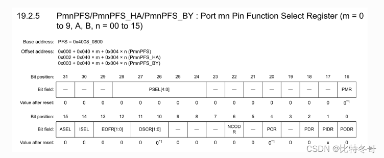
Note: "Pmn" in the above figure, "m = 0 to 9, A, B" indicates the range of IO port m, and "n = 00 to 15" indicates the range of IO pin n.
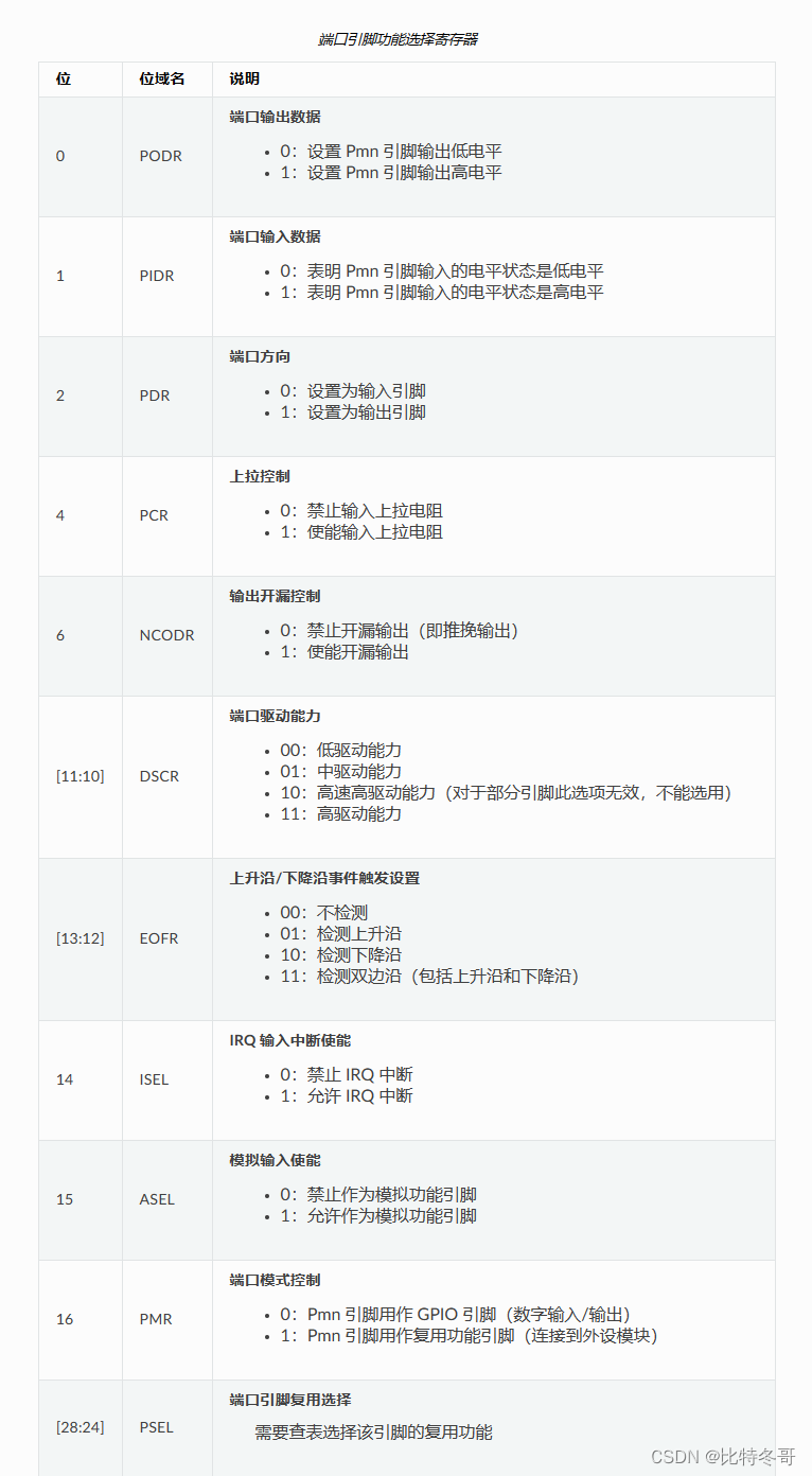
The bit fields of the PmnPFS register are described as follows:
2. Port output data register
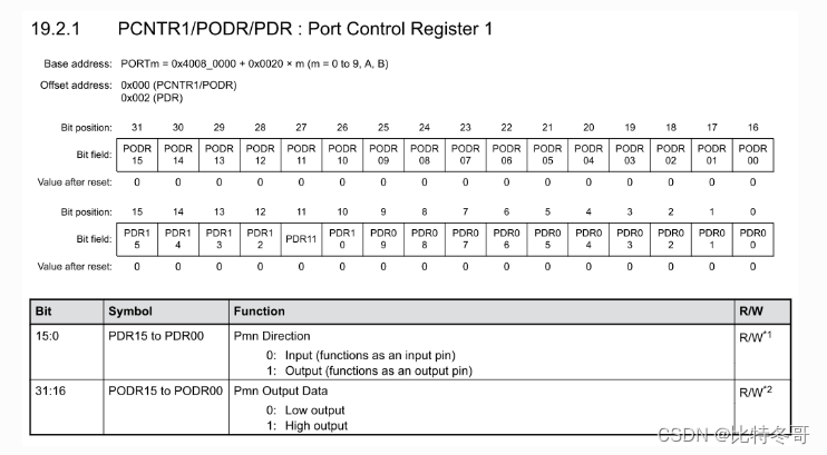
The figure above shows the description of the port output data register. The bit fields of this register are described as follows:
3. Port input data register
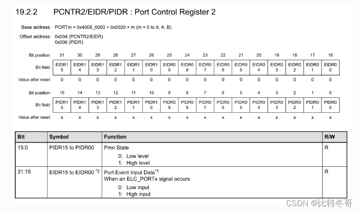
The above figure shows the related description of the port input data register. The bit fields of this register are described as follows:
4. Port output set/reset register
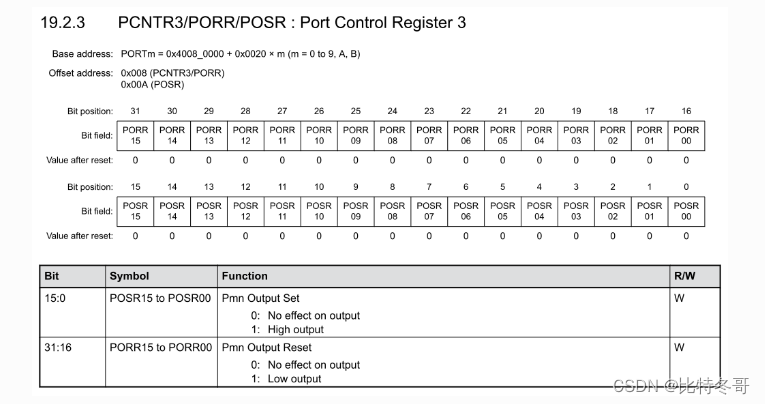
The above figure shows the description of the port output set/reset register. The bit fields of this register are described as follows:
5. Write protection register
When we want to configure the I/O pins of the RA microcontroller, we mainly need to configure the PmnPFS register, but all PmnPFS registers are protected by default, so if we want to write to the PmnPFS register corresponding to the pin Pmn, we need to first pass The write-protect register releases write protection.
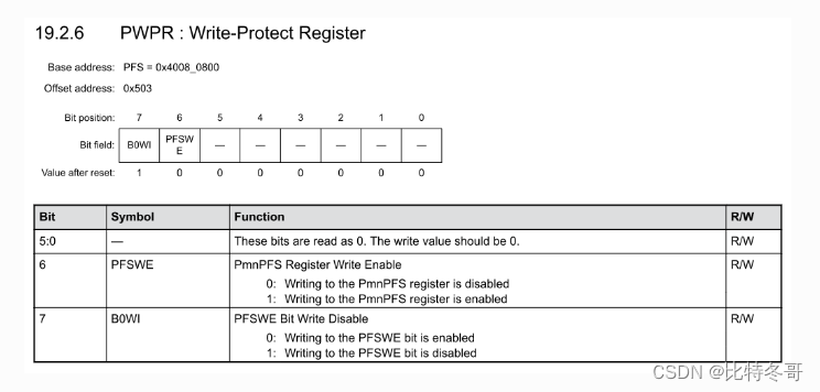
The above figure shows the description of the write protection register. The bit fields of this register are described as follows:
4. Light up the LED light (register)
1. Hardware design
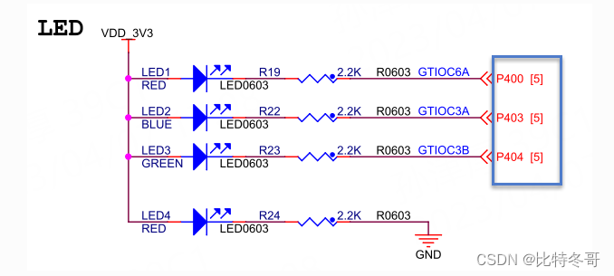
The LED circuit diagram of Wildfire Qiming 6M5 development board is shown in the figure. In the figure, pins P400, P403, and P404 of the RA6M5 chip are respectively connected to the cathodes of LED1, LED2, and LED3 through a 2.2 KΩ current-limiting resistor, and the anodes of the LEDs are connected to the 3.3V power supply. And LED4 is the power indicator light, it will light up as long as the development board is powered on.
2. Software design
Copy a previously created Keil project template "06_Template", then rename the project folder to "08_Register_LED", enter the folder and double-click the Keil project file to open the project.
(1) Register definition header file
When the new project is completed, the header file that defines the register has been automatically included in the project, for example: R7FA6M5BH.h header file. In this header file, all the register definitions of the chip have been included, including the registers of the IOPORT peripheral.
Taking the RA6M5 project of Qiming 6M5 development board as an example, we list the IOPORT partial register definitions here (they exist in the register definition header file R7FA6M5BH.h).
IOPORT section register definition in R7FA6M5BH.h file
/**
  * @brief I/O Ports (R_PORT0)
  */

typedef struct {

                                    /*!< (@ 0x40080000) R_PORT0 Structure                                          */

   union {


      union {


         __IOM uint32_t PCNTR1;                    /*!< (@ 0x00000000) Port Control Register 1                                    */

         struct {


            __IOM uint32_t PDR      : 16;           /*!< [15..0] Pmn Direction                                                     */
            __IOM uint32_t PODR     : 16;           /*!< [31..16] Pmn Output Data                                                  */
         } PCNTR1_b;
      } ;

      struct {


         union {


            __IOM uint16_t PODR;                    /*!< (@ 0x00000000) Output data register                                       */

            /* ... 代码过长省略 ... */
         } ;

         union {


            __IOM uint16_t PDR;                     /*!< (@ 0x00000002) Data direction register                                    */

            /* ... 代码过长省略 ... */
         } ;
      };
   };

   union {


      union {


         __IM  uint32_t PCNTR2;                    /*!< (@ 0x00000004) Port Control Register 2                                    */

         struct {


            __IM  uint32_t PIDR     : 16;           /*!< [15..0] Pmn Input Data                                                    */
            __IM  uint32_t EIDR     : 16;           /*!< [31..16] Pmn Event Input Data                                             */
         } PCNTR2_b;
      } ;

      struct {


         union {


            __IM  uint16_t EIDR;                    /*!< (@ 0x00000004) Event input data register                                  */

            /* ... 代码过长省略 ... */
         } ;

         union {


            __IM  uint16_t PIDR;                    /*!< (@ 0x00000006) Input data register                                        */

            /* ... 代码过长省略 ... */
         } ;
      };
   };

   union {


      union {


         __OM  uint32_t PCNTR3;                    /*!< (@ 0x00000008) Port Control Register 3                                    */

         struct {


            __OM  uint32_t POSR     : 16;           /*!< [15..0] Pmn Output Set                                                    */
            __OM  uint32_t PORR     : 16;           /*!< [31..16] Pmn Output Reset                                                 */
         } PCNTR3_b;
      } ;

      struct {


         union {


            __OM  uint16_t PORR;                    /*!< (@ 0x00000008) Output set register                                        */

            /* ... 代码过长省略 ... */
         } ;

         union {


            __OM  uint16_t POSR;                    /*!< (@ 0x0000000A) Output reset register                                      */

            /* ... 代码过长省略 ... */
         } ;
      };
   };

   union {


      union {


         __IOM uint32_t PCNTR4;                    /*!< (@ 0x0000000C) Port Control Register 4                                    */

         struct {


            __IOM uint32_t EOSR     : 16;           /*!< [15..0] Pmn Event Output Set                                              */
            __IOM uint32_t EORR     : 16;           /*!< [31..16] Pmn Event Output Reset                                           */
         } PCNTR4_b;
      } ;

      struct {


         union {


            __IOM uint16_t EORR;                    /*!< (@ 0x0000000C) Event output set register                                  */

            /* ... 代码过长省略 ... */
         } ;

         union {


            __IOM uint16_t EOSR;                    /*!< (@ 0x0000000E) Event output reset register                                */

            /* ... 代码过长省略 ... */
         } ;
      };
   };
} R_PORT0_Type;                                 /*!< Size = 16 (0x10)                                                          */


/**
  * @brief I/O Ports-PFS (R_PFS)
  */

typedef struct {

                                    /*!< (@ 0x40080800) R_PFS Structure                                            */
   __IOM R_PFS_PORT_Type PORT[15];               /*!< (@ 0x00000000) Port [0..14]                                               */
} R_PFS_Type;                                   /*!< Size = 960 (0x3c0)                                                        */


/**
  * @brief I/O Ports-MISC (R_PMISC)
  */

typedef struct {

                                    /*!< (@ 0x40080D00) R_PMISC Structure                                          */

   union {


      __IOM uint8_t PFENET;                       /*!< (@ 0x00000000) Ethernet Control Register                                  */

      /* ... 代码过长省略 ... */
   } ;
   __IM  uint8_t   RESERVED[2];

   union {


      __IOM uint8_t PWPR;                         /*!< (@ 0x00000003) Write-Protect Register                                     */

      /* ... 代码过长省略 ... */
   } ;
   __IM  uint8_t   RESERVED1;

   union {


      __IOM uint8_t PWPRS;                        /*!< (@ 0x00000005) Write-Protect Register for Secure                          */

      /* ... 代码过长省略 ... */
   } ;
   __IM  uint16_t  RESERVED2[5];
   __IOM R_PMISC_PMSAR_Type PMSAR[12];           /*!< (@ 0x00000010) Port Security Attribution Register                         */
} R_PMISC_Type;                                 /*!< Size = 40 (0x28)                                                          */


/** @addtogroup Device_Peripheral_peripheralAddr
  * @{          外设首地址
  */

#define R_PORT0_BASE                0x40080000UL
#define R_PORT1_BASE                0x40080020UL
#define R_PORT2_BASE                0x40080040UL
#define R_PORT3_BASE                0x40080060UL
#define R_PORT4_BASE                0x40080080UL
#define R_PORT5_BASE                0x400800A0UL
#define R_PORT6_BASE                0x400800C0UL
#define R_PORT7_BASE                0x400800E0UL
#define R_PORT8_BASE                0x40080100UL
#define R_PORT9_BASE                0x40080120UL
#define R_PORT10_BASE               0x40080140UL
#define R_PORT11_BASE               0x40080160UL
#define R_PORT12_BASE               0x40080180UL
#define R_PORT13_BASE               0x400801A0UL
#define R_PORT14_BASE               0x400801C0UL
#define R_PFS_BASE                  0x40080800UL
#define R_PMISC_BASE                0x40080D00UL


/** @addtogroup Device_Peripheral_declaration
  * @{          外设寄存器声明(定义结构体指针,指向 IOPORT 寄存器首地址)
  */

#define R_PORT0                     ((R_PORT0_Type*)           R_PORT0_BASE)
#define R_PORT1                     ((R_PORT0_Type*)           R_PORT1_BASE)
#define R_PORT2                     ((R_PORT0_Type*)           R_PORT2_BASE)
#define R_PORT3                     ((R_PORT0_Type*)           R_PORT3_BASE)
#define R_PORT4                     ((R_PORT0_Type*)           R_PORT4_BASE)
#define R_PORT5                     ((R_PORT0_Type*)           R_PORT5_BASE)
#define R_PORT6                     ((R_PORT0_Type*)           R_PORT6_BASE)
#define R_PORT7                     ((R_PORT0_Type*)           R_PORT7_BASE)
#define R_PORT8                     ((R_PORT0_Type*)           R_PORT8_BASE)
#define R_PORT9                     ((R_PORT0_Type*)           R_PORT9_BASE)
#define R_PORT10                    ((R_PORT0_Type*)           R_PORT10_BASE)
#define R_PORT11                    ((R_PORT0_Type*)           R_PORT11_BASE)
#define R_PORT12                    ((R_PORT0_Type*)           R_PORT12_BASE)
#define R_PORT13                    ((R_PORT0_Type*)           R_PORT13_BASE)
#define R_PORT14                    ((R_PORT0_Type*)           R_PORT14_BASE)
#define R_PFS                       ((R_PFS_Type*)             R_PFS_BASE)
#define R_PMISC                     ((R_PMISC_Type*)           R_PMISC_BASE)
3. The hal_entry entry function
Generally speaking, we should write our program in the main function next, but it is different when using the FSP library. In the case of not using RTOS, it stipulates that the function named hal_entry is used as the user application program entry, so we should write our code under the entry function of hal_entry.
In fact, when using RTOS, the program starts thread scheduling from the main function; when not using RTOS, the main function of the entry function of the C language program calls the hal_entry function. Our new project does not use RTOS, so the user program is executed from the hal_entry function. We open the "\src\hal_entry.c" file and write our code in the hal_entry function.
Taking the Qiming 6M5 development board as an example, the hal_entry function code of the RA6M5 project is as follows.
hal_entry.c file
 void hal_entry(void)
 {


     /* TODO: add your own code here */

     /* 取消写保护 */
     R_PMISC->PWPR = 0;                               ///< Clear BOWI bit - writing to PFSWE bit enabled
     R_PMISC->PWPR = 1U << BSP_IO_PWPR_PFSWE_OFFSET;  ///< Set PFSWE bit - writing to PFS register enabled

     /* LED1:配置引脚 P400 对应的PFS寄存器 */
     R_PFS->PORT[BSP_IO_PORT_04_PIN_00>>8].PIN[BSP_IO_PORT_04_PIN_00 & 0xFF].PmnPFS =
        IOPORT_CFG_PORT_DIRECTION_OUTPUT | IOPORT_CFG_PORT_OUTPUT_LOW;
     /* LED2:配置引脚 P403 对应的PFS寄存器 */
     R_PFS->PORT[BSP_IO_PORT_04_PIN_03>>8].PIN[BSP_IO_PORT_04_PIN_03 & 0xFF].PmnPFS =
        IOPORT_CFG_PORT_DIRECTION_OUTPUT | IOPORT_CFG_PORT_OUTPUT_LOW;
     /* LED3:配置引脚 P404 对应的PFS寄存器 */
     R_PFS->PORT[BSP_IO_PORT_04_PIN_04>>8].PIN[BSP_IO_PORT_04_PIN_04 & 0xFF].PmnPFS =
        IOPORT_CFG_PORT_DIRECTION_OUTPUT | IOPORT_CFG_PORT_OUTPUT_LOW;

     /** 此时3个LED灯的引脚默认输出的是低电平
      *  所以3个LED灯都会默认亮起来
      *  我们在 while 循环里让 LED1 闪烁:每秒钟翻转一次状态
      */

     while(1)
     {


        /* 翻转LED灯:LED1 */
        //R_PORT4->PODR |= 1<<(BSP_IO_PORT_04_PIN_00 & 0xFF);
        //R_BSP_SoftwareDelay(1000, BSP_DELAY_UNITS_MILLISECONDS);
        //R_PORT4->PODR &= (uint16_t)~(1 << (BSP_IO_PORT_04_PIN_00 & 0xFF));
        //R_BSP_SoftwareDelay(1000, BSP_DELAY_UNITS_MILLISECONDS);

        /* 或者也可以这样用位异或操作来翻转LED1 */
        R_PORT4->PODR ^= 1<<(BSP_IO_PORT_04_PIN_00 & 0xFF);
        R_BSP_SoftwareDelay(1000, BSP_DELAY_UNITS_MILLISECONDS);
     }

     //这后面的代码无需理会
 #if BSP_TZ_SECURE_BUILD
     /* Enter non-secure code */
     R_BSP_NonSecureEnter();
 #endif
 }
4. Download and verify
After writing the above code, compile and download the program to the development board, press the reset button to reset the development board, and you can observe that there are two of the three LED lights on the development board except the power indicator. The light stays on and one light blinks slowly. The blinking LED is LED1, which changes its on and off state every second (1000 milliseconds).