Abstract: I believe that everyone has a good understanding of the NB-IoT communication expansion board of the bear faction, but have you really understood its internal structure? Today, the editor will not talk about technology, and I will take you to dismantle, machine and guest!
I believe everyone has a good understanding of the NB-IoT communication expansion board of the bear faction, but have you really understood its internal structure ? Today, the editor will not talk about technology, and I will take you to dismantle, machine and guest !
Disassembly object: BC35-G communication module
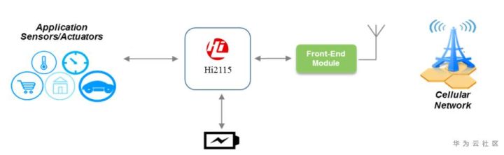
BC35-G module is a NB-IoT communication module based on HiSilicon Hi2115 (also known as Boudica150) chip released by Quectel . BC35-G supports the following two operating modes: NB-IoT+MCU mode and OpenCPU mode.
NB-IoT+MCU mode is one of our common combination methods (Little Bear Pie IoT is this combination method). MCU is used as the main control for data collection and control, and the MCU sends AT commands to the module to realize the device and the Internet Data interaction. OpenCPU uses the module's own processing capabilities to complete the work of the MCU, thereby eliminating the need for the MCU.
Let us take off its "coat" and take a look at its internal structure

Today's protagonist is the biggest chip: Hi2115. Next, the editor will conduct an in-depth analysis of this NB-IoT chip.
Hi2115 is the second NB-IoT communication chip developed by Huawei HiSilicon (the first is Hi2110), with a main frequency of 48MHz, 352KB Flash, 64KB RAM, supporting the 3GPP R14 standard, and operating at 698-960 MHz and 1695-2180 MHz. Working within the range, the system bandwidth is 200 kHz.
Next, from the shallower to the deeper, explore its deepest "secret" through the appearance of this chip.
The Hi2115 chip has three processor subsystems to separate different functions, facilitate authentication and simplify third-party application development.
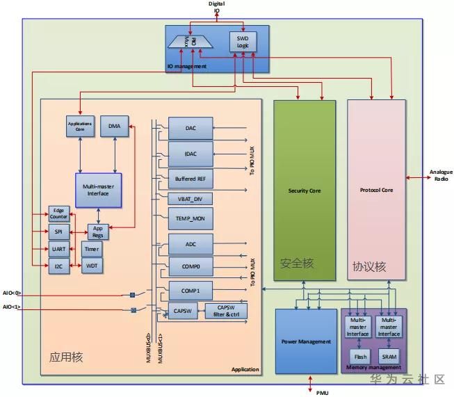
Internal structure block diagram of Hi2115 chip
The three processor subsystems of the Hi2115 chip are:
1. Application core processor (Application): Application core supports users to execute third-party application codes on applications
2. Security Core Processor (Security Core): The security core maintains the security and integrity of Hi2115 by verifying the code running on the system. It also generates random numbers and controls the memory access of the other two cores.
3. Protocol core processor (Protocol Core): The protocol core acts as a communication processor and forms the basis for realizing all layers of the communication protocol stack. It includes a dedicated ARM Cortex M0 core and a Dual-MAC DSP with dedicated on-chip RAM. There is a USIM interface to allow operation with an external SIM, and a MIPI RFFE interface to interface with an external radio frequency circuit.
Between the three sub-processors, data sharing is achieved through memory sharing. Each core operates independently without interference with each other. Application verification can safely release all user permissions for user-side APP development.
The Hi2115 chip has three working modes, which determine the available functions of different power saving levels.
1. Active mode (Active)
In this mode, all the functions of the chip are available, and all processors are running normally. Both radio transmission and reception are performed in this mode. At the same time, standby mode and deep sleep mode can only be switched in active mode.
2. Standby mode (Standby)
In standby mode, all processors are in an inactive state, but all peripheral devices (including DMA and embedded Flash) are in an active state. The system clock is active and reduces power consumption through clock gating and power gating. When all processors execute the wait for interrupt (WFI) instruction, they enter the standby mode.
3. Deep-Sleep mode (Deep-Sleep)
When in this mode, only 32.768kHz RTC and certain peripherals operate. The chip can send messages through RTC interrupts or external events from peripheral devices to wake up modules in deep sleep mode. This mode requires all processor inputs to be set to deep sleep mode to enter, and then execute the wait for interrupt (WFI) instruction.
After exploring the framework, let’s learn more about the peripherals of the Hi2115 chip:
- 1 universal UART (up to 1.5Mbit/s)
- 2 low power UARTs (support asynchronous operation under low power consumption)
- 2 IIC (up to 1Mbit/s)
- 2 SPI (up to 24Mbit/s)
- 1 10bit ADC (818 ksps)
- 1 10bit DAC
- 1 high-speed analog comparator
- 22 programmable IO (configurable)
Among the 40 PIOs of the Hi2115 chip, 24 PIOs are available on the application core. The IO pin functions of each PIO are controlled by software, including: direction, interrupt configuration, drive strength, and integrated pull-up and pull-down resistors.
After understanding the above, do you have the feeling of seeing the moonlight when you see through the clouds and mist? Let us continue to analyze the internal architecture of the chip with this feel .
- Chip power supply
Hi2115 chip is powered by a single power supply, dual-mode (PWM / PFM) buck regulator SMPSU powers the digital core and is optimized for the current of deep sleep. The integrated linear regulator provides analog and radio power rails to achieve high transmit power and isolate noise interference. These linear regulators are powered by a second on-chip SMPSU to improve power consumption efficiency, and in order to reduce power consumption, the chip can automatically disable the internal radio power rail. - The reference clock
Hi2115 requires a low phase noise reference clock to provide a frequency reference for the PLL and ADC, and the chip also requires a 32.768 kHz crystal oscillator for timing and deep sleep wake-up. The processor is driven by an internally generated clock and does not rely on two reference clocks to start. - RF function
The radio of the Hi2115 chip is used for NB-IoT communication at cellular frequencies. There are two differential LNA inputs with 100Ω impedance that can be configured by external components for LB (low frequency band 698-960 MHz) and MB (medium frequency band 1695-2180 MHz). The transmitter has two single-ended outputs with an impedance of 50Ω, one for LB and the other for MB.
There are the following components between the transceiver RF port and the antenna:
1.TX power amplifier
This is a PA capable of producing 23 dBm output power, with a gain of 20-30 dB and sufficient linearity to meet 3GPP requirements.
2.TX harmonic filter
Its specifications depend on the choice of PA. In some cases, it may be integrated into the PA and does not need to be used separately.
3.TX/RX switch
The RF switch connects the antenna to the PA output and RX input. This switch can be controlled by one or more PIOs of Hi2115.
4. RX harmonic filter
Device used to filter one or more harmonics in power system
5.RX matching components / balun
The Hi2115 chip also supports MIPI RFFE interfaces v1.0 and v2.0, which are used to control power amplifiers and RF front-end modules that support 1.8V interfaces, and the supported SCLK frequency range is 32kHz~26MHz.
Click to follow and learn about Huawei Cloud's fresh technology for the first time~