Q:还有一种RC corner 带后缀『_T』,只用于setup signoff,T指的是什么?
A:T代表tighten,在rc的variation上的sigma分布比不带T的更紧,因此只能用于setup,hold不推荐。Appleto Apple地比较,T的variation更小,理论看到的rc变化更小,单从setup产生violation的可能性更小。至于悲观还是乐观,除非自己定criteria,其余的follow foundry或者vendor的rule最重要。
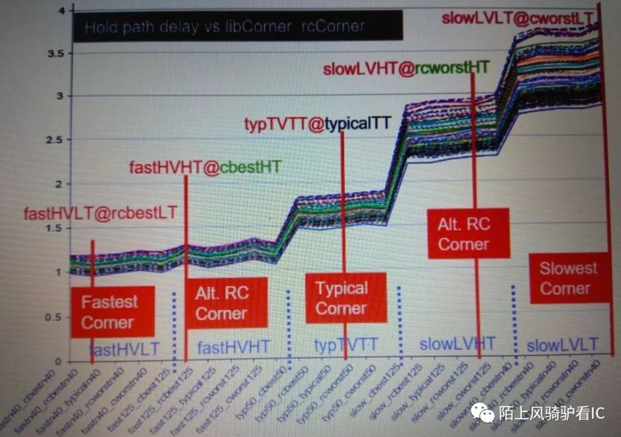
Q:为什么setup既需要sign-off C-corner又需要sign-offRC-corner?
A:因为C-corner表示『电容』最大/最小,而RC-corner是『电容*电阻』最大/最小。通常对于短线而言,电容占主导地位,C-corner可以cover RC-corner,但对于长线则电阻占主导地位,C-corner无法cover RC-corner,而是反过来RC-corner去cover C-corner。而没人保证一个设计里只有短线没有长线,也没权威对长短的幅度有量化的定义,所以最保险的就是两者分别sign-off。
Q:为什么hold需要sign-off所有的corner?
A:对于hold而言,根据其仿真曲线,相互之间都无法完全覆盖,故需要sign-off所有corner。
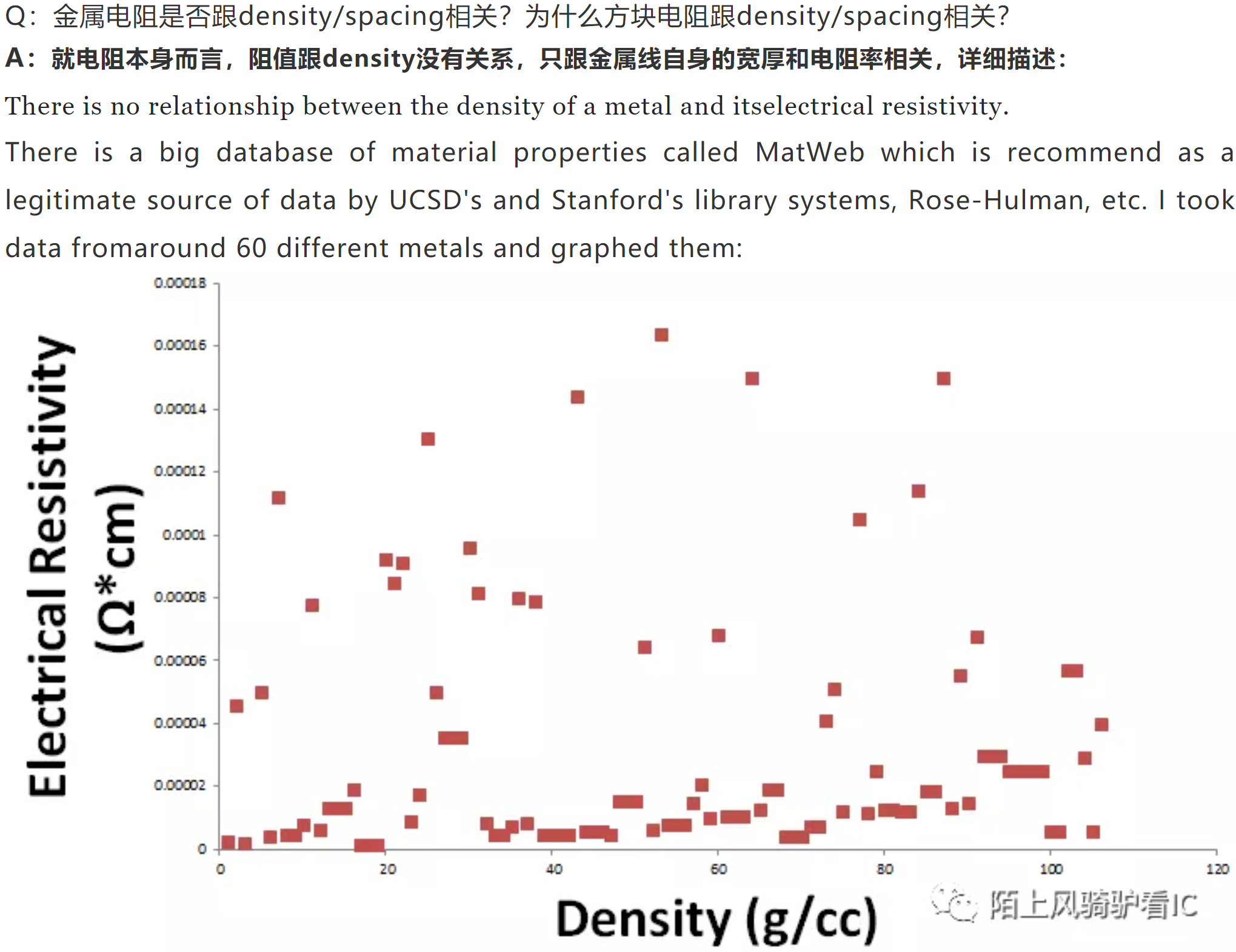
As you can see there is no empirical relationship. From a theoryperspective, density has to do with atomic packing and resistivity has to dowith electronic structure.
Iwill admit, however, that gaseous copper is an extremely poor conductor.
但是,在半导体制造过程中,由于工艺偏差,电阻跟金属线的density是相关的。此时,电阻率是线宽跟线间距的函数。这一关系,在foundry给的工艺文件里都有相应的描述,这些都是在抽RC时需要考虑的因素。
Resistivity as a Function of Width and Spacing (Rs = f(W) or rho=f(W,S))
Variationin resistivity is caused by a number of phenomena. Copper is a softer materialthan the dielectric in which it is embedded. As a result, the polishing of thewafer during the CMP process has a tendency to remove a little extra copperfrom the top of the wire. This effect is called dishing because of the shape ofthe resulting wire top. The effect becomes more pronounced as the wire widthincreases. This effect is shown in exaggerated form in following pic.
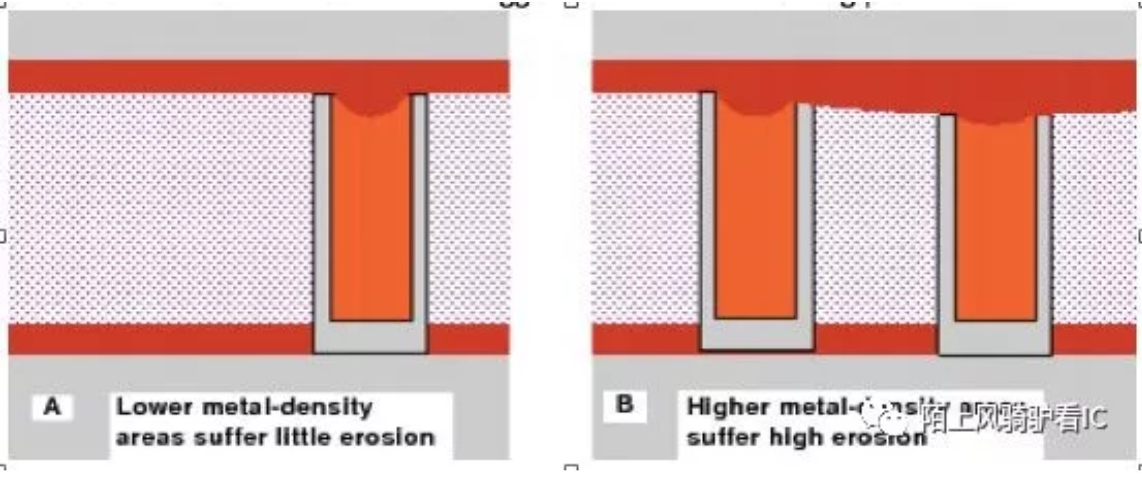
To reduce theeffect of dishing on wide wires, small holes, or slots, can be inserted atregular intervals in wide wires. These slots insert a form of hard"posts" in the wire so that the CMP process removes less copper. Thistechnique reduces the dishing, as well as the effective resistivity.
Anothercontributor to resistivity variation is the cladding in copper wires. Claddingis the material grown around the sides and bottom of copper wires to protectthem from chemical reactions with the dielectric material. This cladding isillustrated in gray in following pic. The thickness ofthe cladding on the sides and bottoms of wires also varies with the width of awire. Because cladding has a much higher resistance than copper, it impacts theeffective resistivity of copper wires. This effect is more pronounced in thenarrowest wires. The combination of the effects ofdishing, slotting, and cladding thickness is modeled by the wire resistivity asa function of the wire width in silicon, and its spacing.
A:就电阻本身是跟spacing没有无关的,但在半导体制造过程中,因为铜软,所以在dishing时会把铜线切掉一些,这跟那个范围的金属线密度相关,而且这个关系好像也不是线性的。线的密度不同,会使得制造过程对线的厚度造成的影响不同,线厚度被改变了,那阻值自然被改变了。在QRC抽RC的时候会把这一效应模拟成『电阻率=f(W,S)』。 这一效应在foundry给的工艺文件里有相应的描述。
@SteveB 后端角度?如果讲RC 后端抽怎么考虑,讲好原理以后剩下的就是按照RC corner 加上温度抽,交给工具。如果想要知道原理,有几个方面可以去考虑,也是一般后端拿到新工艺需要去研究的:
-
对于寄生参数提取,相关的各个工具的技术文件怎么来?
-
每个corner下的配合PVT signoff里的T趋势如何,是否可以对signoff做精简 ?
-
double pattern multiple pattern 的影响如何?
-
研究DFM。
Q:为什么dpt之后多了ccworst跟ccbest?
A:@Fred ccbest和ccworst的出现是因为dpt同层metal分两张mask,两张mask的alignment误差会导致两张mask上相邻的走线的间距变化,而造成电容的变化