开发环境:win10 64位 + VMware12 + Ubuntu14.04 32位
工具链:linaro提供的gcc-linaro-6.1.1-2016.08-x86_64_arm-linux-gnueabi
要移植的u-boot版本:u-boot-2016-11
Tiny4412开发板硬件版本为:
底板: Tiny4412SDK 1312B
核心板:Tiny4412 - 1306
1、原理图
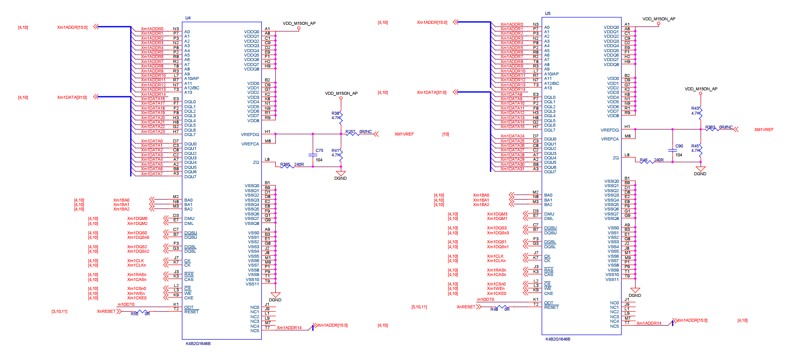
从原理图上可以看出,4颗ddr3@16bit,用到一个控制器两个片选(chip0,chip1).共1G
2,DDR3初始化代码
diff --git a/arch/arm/mach-exynos/Makefile b/arch/arm/mach-exynos/Makefil
index 5575adf..5889802 100644
--- a/arch/arm/mach-exynos/Makefile
+++ b/arch/arm/mach-exynos/Makefile
@@ -15,7 +15,7 @@ ifdef CONFIG_SPL_BUILD
 obj-$(CONFIG_EXYNOS5)  += clock_init_exynos5.o
 obj-$(CONFIG_EXYNOS5)  += dmc_common.o dmc_init_ddr3.o
 obj-$(CONFIG_EXYNOS4210)+= dmc_init_exynos4.o clock_init_exynos4.o
-obj-$(CONFIG_EXYNOS4412)+= dmc_init_exynos4.o clock_init_exynos4412.o
+obj-$(CONFIG_EXYNOS4412)+= dmc_init_exynos4412.o clock_init_exynos4412.o

 obj-y  += spl_boot.o tzpc.o
 obj-y  += lowlevel_init.o
diff --git a/arch/arm/mach-exynos/dmc_init_exynos4412.c b/arch/arm/mach-e
new file mode 100644
index 0000000..b2c0c0d
--- /dev/null
+++ b/arch/arm/mach-exynos/dmc_init_exynos4412.c
@@ -0,0 +1,254 @@
+/*^M
+ * Memory setup for board based on EXYNOS4412^M
+ *^M
+ *                 2016^M
+ * Modified by AP0904225 <[email protected]>^M
+ *^M
+ * Copyright (C) 2013 Samsung Electronics^M
+ * Rajeshwari Shinde <[email protected]>^M
+ *^M
+ * See file CREDITS for list of people who contributed to this^M
+ * project.^M
+ *^M
+ * This program is free software; you can redistribute it and/or^M
+ * modify it under the terms of the GNU General Public License as^M
+ * published by the Free Software Foundation; either version 2 of^M
+ * the License, or (at your option) any later version.^M
+ *^M
+ * This program is distributed in the hope that it will be useful,^M
+ * but WITHOUT ANY WARRANTY; without even the implied warranty of^M
+ * MERCHANTABILITY or FITNESS FOR A PARTICULAR PURPOSE.  See the^M
+ * GNU General Public License for more details.^M
+ *^M
+ * You should have received a copy of the GNU General Public License^M
+ * along with this program; if not, write to the Free Software^M
+ * Foundation, Inc., 59 Temple Place, Suite 330, Boston,^M
+ * MA 02111-1307 USA^M
+ */^M
+^M
+#include <config.h>^M
+#include <asm/arch/dmc.h>^M
+#include "common_setup.h"^M
+#include "exynos4412_setup.h"^M
+^M
+#ifdef TINY4412^M
+struct mem_timings mem = {^M
+   .direct_cmd_msr = {^M
+       DIRECT_CMD1, DIRECT_CMD2, DIRECT_CMD3, DIRECT_CMD4^M
+   },^M
+   .timingref   = 0x000000BB,^M
+   .timingrow   = 0x4046654f,^M
+   .timingdata  = 0x46400506,^M
+   .timingpower = 0x52000A3C,^M
+   .zqcontrol   = 0xE3854C03,^M
+   .control0    = 0x71101008,^M
+   .control1    = 0xe0000086,^M
+   .control2    = 0x00000000,^M
+   .concontrol  = 0x0FFF301A,^M
+   .prechconfig = 0xff000000,^M
+   .memcontrol  = 0x00312640,      /* Tiny4412-1412 core board only use
+   .memconfig0  = 0x40e01333,      /* ROW is 15bit */^M
+   .memconfig1  = 0x60e01333,      /* DMC0 address up to 0x7FFFFFFF */^M
+   .dll_resync  = FORCE_DLL_RESYNC,^M
+   .dll_on      = DLL_CONTROL_ON,^M
+^M
+};^M
+#else^M
+struct mem_timings mem = {^M
+   .direct_cmd_msr = {^M
+       DIRECT_CMD1, DIRECT_CMD2, DIRECT_CMD3, DIRECT_CMD4^M
+   },^M
+   .timingref = TIMINGREF_VAL,^M
+   .timingrow = TIMINGROW_VAL,^M
+   .timingdata = TIMINGDATA_VAL,^M
+   .timingpower = TIMINGPOWER_VAL,^M
+   .zqcontrol = ZQ_CONTROL_VAL,^M
+   .control0 = CONTROL0_VAL,^M
+   .control1 = CONTROL1_VAL,^M
+   .control2 = CONTROL2_VAL,^M
+   .concontrol = CONCONTROL_VAL,^M
+   .prechconfig = PRECHCONFIG,^M
+   .memcontrol = MEMCONTROL_VAL,^M
+   .memconfig0 = MEMCONFIG0_VAL,^M
+   .memconfig1 = MEMCONFIG1_VAL,^M
+   .dll_resync = FORCE_DLL_RESYNC,^M
+   .dll_on = DLL_CONTROL_ON,^M
+};^M
+#endif^M
+^M
+static void phy_control_reset(int ctrl_no, struct exynos4_dmc *dmc)^M
+{^M
+   if (ctrl_no) {^M
+       writel((mem.control1 | (1 << mem.dll_resync)),^M
+              &dmc->phycontrol1);^M
+       writel((mem.control1 | (0 << mem.dll_resync)),^M
+              &dmc->phycontrol1);^M
+   } else {^M
+       writel((mem.control0 | (0 << mem.dll_on)),^M
+              &dmc->phycontrol0);^M
+       writel((mem.control0 | (1 << mem.dll_on)),^M
+              &dmc->phycontrol0);^M
+   }^M
+}^M
+^M
+static void dmc_config_mrs(struct exynos4_dmc *dmc, int chip)^M
+{^M
+   int i;^M
+   unsigned long mask = 0;^M
+^M
+   if (chip)^M
+       mask = DIRECT_CMD_CHIP1_SHIFT;^M
+^M
+   for (i = 0; i < MEM_TIMINGS_MSR_COUNT; i++) {^M
+       writel(mem.direct_cmd_msr[i] | mask,^M
+              &dmc->directcmd);^M
+   }^M
+}^M
+^M
+static void dmc_init(struct exynos4_dmc *dmc)^M
+{^M
+   /*^M
+    * DLL Parameter Setting:^M
+    * Termination: Enable R/W^M
+    * Phase Delay for DQS Cleaning: 180' Shift^M
+    */^M
+   writel(mem.control1, &dmc->phycontrol1);^M
+^M
+   /*^M
+    * ZQ Calibration^M
+    * Termination: Disable^M
+    * Auto Calibration Start: Enable^M
+    */^M
+   writel(mem.zqcontrol, &dmc->phyzqcontrol);^M
+   sdelay(0x100000);^M
+^M
+   /*^M
+    * Update DLL Information:^M
+    * Force DLL Resyncronization^M
+    */^M
+   phy_control_reset(1, dmc);^M
+   phy_control_reset(0, dmc);^M
+^M
+   /* Set DLL Parameters */^M
+   writel(mem.control1, &dmc->phycontrol1);^M
+^M
+   /* DLL Start */^M
+   writel((mem.control0 | CTRL_START | CTRL_DLL_ON), &dmc->phycontrol0);
+^M
+   writel(mem.control2, &dmc->phycontrol2);^M
+^M
+   /* Set Clock Ratio of Bus clock to Memory Clock */^M
+   writel(mem.concontrol, &dmc->concontrol);^M
+^M
+   /*^M
+    * Memor Burst length: 8^M
+    * Number of chips: 2^M
+    * Memory Bus width: 32 bit^M
+    * Memory Type: DDR3^M
+    * Additional Latancy for PLL: 1 Cycle^M
+    */^M
+   writel(mem.memcontrol, &dmc->memcontrol);^M
+^M
+   writel(mem.memconfig0, &dmc->memconfig0);^M
+   writel(mem.memconfig1, &dmc->memconfig1);^M
+/*^M
+#ifdef TINY4412^M
+   writel(0x8000001F, &dmc->ivcontrol);^M
+#endif^M
+*/^M
+   /* Config Precharge Policy */^M
+   writel(mem.prechconfig, &dmc->prechconfig);^M
+   /*^M
+    * TimingAref, TimingRow, TimingData, TimingPower Setting:^M
+    * Values as per Memory AC Parameters^M
+    */^M
+   writel(mem.timingref, &dmc->timingref);^M
+   writel(mem.timingrow, &dmc->timingrow);^M
+   writel(mem.timingdata, &dmc->timingdata);^M
+   writel(mem.timingpower, &dmc->timingpower);^M
+^M
+   /* Chip0: NOP Command: Assert and Hold CKE to high level */^M
+   writel(DIRECT_CMD_NOP, &dmc->directcmd);^M
+   sdelay(0x100000);^M
+^M
+   /* Chip0: EMRS2, EMRS3, EMRS, MRS Commands Using Direct Command */^M
+   dmc_config_mrs(dmc, 0);^M
+   sdelay(0x100000);^M
+^M
+   /* Chip0: ZQINIT */^M
+   writel(DIRECT_CMD_ZQ, &dmc->directcmd);^M
+   sdelay(0x100000);^M
+^M
+//#ifndef TINY4412^M
+   /* Chip1: NOP Command: Assert and Hold CKE to high level */^M
+   writel((DIRECT_CMD_NOP | DIRECT_CMD_CHIP1_SHIFT), &dmc->directcmd);^M
+   sdelay(0x100000);^M
+^M
+   /* Chip1: EMRS2, EMRS3, EMRS, MRS Commands Using Direct Command */^M
+   dmc_config_mrs(dmc, 1);^M
+   sdelay(0x100000);^M
+^M
+   /* Chip1: ZQINIT */^M
+   writel((DIRECT_CMD_ZQ | DIRECT_CMD_CHIP1_SHIFT), &dmc->directcmd);^M
+   sdelay(0x100000);^M
+//#endif^M
+^M
+   phy_control_reset(1, dmc);^M
+   sdelay(0x100000);^M
+^M
+   /* turn on DREX0, DREX1 */^M
+   writel((mem.concontrol | AREF_EN), &dmc->concontrol);^M
+}^M
+^M
+void mem_ctrl_init(int reset)^M
+{^M
+   struct exynos4_dmc *dmc;^M
+^M
+   /*^M
+    * Async bridge configuration at CPU_core:^M
+    * 1: half_sync^M
+    * 0: full_sync^M
+    */^M
+   writel(1, ASYNC_CONFIG);^M
+^M
+#ifndef TINY4412^M
+#ifdef CONFIG_ORIGE^M
+   /* Interleave: 2Bit, Interleave_bit1: 0x15, Interleave_bit0: 0x7 */^M
+   writel(APB_SFR_INTERLEAVE_CONF_VAL, EXYNOS4_MIU_BASE ^M
+       APB_SFR_INTERLEAVE_CONF_OFFSET);^M
+   /* Update MIU Configuration */^M
+   writel(APB_SFR_ARBRITATION_CONF_VAL, EXYNOS4_MIU_BASE ^M
+       APB_SFR_ARBRITATION_CONF_OFFSET);^M
+#else^M
+   writel(APB_SFR_INTERLEAVE_CONF_VAL, EXYNOS4_MIU_BASE ^M
+       APB_SFR_INTERLEAVE_CONF_OFFSET);^M
+   writel(INTERLEAVE_ADDR_MAP_START_ADDR, EXYNOS4_MIU_BASE ^M
+       ABP_SFR_INTERLEAVE_ADDRMAP_START_OFFSET);^M
+   writel(INTERLEAVE_ADDR_MAP_END_ADDR, EXYNOS4_MIU_BASE ^M
+       ABP_SFR_INTERLEAVE_ADDRMAP_END_OFFSET);^M
+   writel(INTERLEAVE_ADDR_MAP_EN, EXYNOS4_MIU_BASE ^M
+       ABP_SFR_SLV_ADDRMAP_CONF_OFFSET);^M
+#ifdef CONFIG_MIU_LINEAR^M
+   writel(SLAVE0_SINGLE_ADDR_MAP_START_ADDR, EXYNOS4_MIU_BASE ^M
+       ABP_SFR_SLV0_SINGLE_ADDRMAP_START_OFFSET);^M
+   writel(SLAVE0_SINGLE_ADDR_MAP_END_ADDR, EXYNOS4_MIU_BASE ^M
+       ABP_SFR_SLV0_SINGLE_ADDRMAP_END_OFFSET);^M
+   writel(SLAVE1_SINGLE_ADDR_MAP_START_ADDR, EXYNOS4_MIU_BASE ^M
+       ABP_SFR_SLV1_SINGLE_ADDRMAP_START_OFFSET);^M
+   writel(SLAVE1_SINGLE_ADDR_MAP_END_ADDR, EXYNOS4_MIU_BASE ^M
+       ABP_SFR_SLV1_SINGLE_ADDRMAP_END_OFFSET);^M
+   writel(APB_SFR_SLV_ADDR_MAP_CONF_VAL, EXYNOS4_MIU_BASE ^M
+       ABP_SFR_SLV_ADDRMAP_CONF_OFFSET);^M
+#endif^M
+#endif^M
+#endif^M
+^M
+   /* DREX0 */^M
+   dmc = (struct exynos4_dmc *)samsung_get_base_dmc_ctrl();^M
+   dmc_init(dmc);^M
+^M
+   /* DREX1 */^M
+   dmc = (struct exynos4_dmc *)(samsung_get_base_dmc_ctrl()^M
+                +DMC_OFFSET);^M
+   dmc_init(dmc);^M
+}^M
diff --git a/arch/arm/mach-exynos/exynos4412_setup.h b/arch/arm/mach-exyn
index 11e9d09..fced9a8 100644
--- a/arch/arm/mach-exynos/exynos4412_setup.h
+++ b/arch/arm/mach-exynos/exynos4412_setup.h

+/* Bus Configuration Register Address */^M
+#define ASYNC_CONFIG       0x10010350^M
+^M
+/* DMC */^M
+#define DIRECT_CMD_NOP 0x07000000^M
+#define DIRECT_CMD_ZQ  0x0a000000^M
+#define DIRECT_CMD_CHIP1_SHIFT (1 << 20)^M
+#define MEM_TIMINGS_MSR_COUNT  4^M
+#define CTRL_START (1 << 0)^M
+#define CTRL_DLL_ON    (1 << 1)^M
+#define AREF_EN        (1 << 5)^M
+#define DRV_TYPE   (1 << 6)^M
+^M
+struct mem_timings {^M
+   unsigned direct_cmd_msr[MEM_TIMINGS_MSR_COUNT];^M
+   unsigned timingref;^M
+   unsigned timingrow;^M
+   unsigned timingdata;^M
+   unsigned timingpower;^M
+   unsigned zqcontrol;^M
+   unsigned control0;^M
+   unsigned control1;^M
+   unsigned control2;^M
+   unsigned concontrol;^M
+   unsigned prechconfig;^M
+   unsigned memcontrol;^M
+   unsigned memconfig0;^M
+   unsigned memconfig1;^M
+   unsigned dll_resync;^M
+   unsigned dll_on;^M
+};^M
+^M
+/* MIU */^M
+/* MIU Config Register Offsets*/^M
+#define APB_SFR_INTERLEAVE_CONF_OFFSET 0x400^M
+#define APB_SFR_ARBRITATION_CONF_OFFSET    0xC00^M
+#define ABP_SFR_SLV_ADDRMAP_CONF_OFFSET    0x800^M
+#define ABP_SFR_INTERLEAVE_ADDRMAP_START_OFFSET    0x808^M
+#define ABP_SFR_INTERLEAVE_ADDRMAP_END_OFFSET  0x810^M
+#define ABP_SFR_SLV0_SINGLE_ADDRMAP_START_OFFSET   0x818^M
+#define ABP_SFR_SLV0_SINGLE_ADDRMAP_END_OFFSET 0x820^M
+#define ABP_SFR_SLV1_SINGLE_ADDRMAP_START_OFFSET   0x828^M
+#define ABP_SFR_SLV1_SINGLE_ADDRMAP_END_OFFSET 0x830^M
+^M
+^M
+#ifdef TINY4412^M
+/* Interleave: 2Bit, Interleave_bit1: 0x15, Interleave_bit0: 0x7 */^M
+#define APB_SFR_INTERLEAVE_CONF_VAL    0x20001507^M
+#define APB_SFR_ARBRITATION_CONF_VAL   0x00000001^M
+#endif^M
+^M
+#define INTERLEAVE_ADDR_MAP_START_ADDR 0x40000000^M
+#define INTERLEAVE_ADDR_MAP_END_ADDR   0xbfffffff^M
+#define INTERLEAVE_ADDR_MAP_EN     0x00000001^M
+^M
+#ifdef CONFIG_MIU_1BIT_INTERLEAVED^M
+/* Interleave_bit0: 0xC*/^M
+#define APB_SFR_INTERLEAVE_CONF_VAL    0x0000000c^M
+#endif^M
+#ifdef CONFIG_MIU_2BIT_INTERLEAVED^M
+/* Interleave: 2Bit, Interleave_bit1: 0x15, Interleave_bit0: 0xc */^M
+#define APB_SFR_INTERLEAVE_CONF_VAL    0x2000150c^M
+#endif^M
+#define SLAVE0_SINGLE_ADDR_MAP_START_ADDR  0x40000000^M
+#define SLAVE0_SINGLE_ADDR_MAP_END_ADDR        0x7fffffff^M
+#define SLAVE1_SINGLE_ADDR_MAP_START_ADDR  0x80000000^M
+#define SLAVE1_SINGLE_ADDR_MAP_END_ADDR        0xbfffffff^M
+/* Enable SME0 and SME1*/^M
+#define APB_SFR_SLV_ADDR_MAP_CONF_VAL      0x00000006^M
+^M
+#define FORCE_DLL_RESYNC   3^M
+#define DLL_CONTROL_ON     1^M
+^M
+#define DIRECT_CMD1    0x00020000^M
+#define DIRECT_CMD2    0x00030000^M
+#define DIRECT_CMD3    0x00010002^M
+#define DIRECT_CMD4    0x00000328^M
+^M
+#define CTRL_ZQ_MODE_NOTERM    (0x1 << 0)^M
+#define CTRL_ZQ_START      (0x1 << 1)^M
+#define CTRL_ZQ_DIV        (0 << 4)^M
+#define CTRL_ZQ_MODE_DDS   (0x7 << 8)^M
+#define CTRL_ZQ_MODE_TERM  (0x2 << 11)^M
+#define CTRL_ZQ_FORCE_IMPN (0x5 << 14)^M
+#define CTRL_ZQ_FORCE_IMPP (0x6 << 17)^M
+#define CTRL_DCC       (0xE38 << 20)^M
+#define ZQ_CONTROL_VAL     (CTRL_ZQ_MODE_NOTERM | CTRL_ZQ_START\^M
+               | CTRL_ZQ_DIV | CTRL_ZQ_MODE_DDS\^M
+               | CTRL_ZQ_MODE_TERM | CTRL_ZQ_FORCE_IMPN\^M
+               | CTRL_ZQ_FORCE_IMPP | CTRL_DCC)^M
+^M
+#define ASYNC          (0 << 0)^M
+#define CLK_RATIO      (1 << 1)^M
+#define DIV_PIPE       (1 << 3)^M
+#define AWR_ON         (1 << 4)^M
+#define AREF_DISABLE       (0 << 5)^M
+#define DRV_TYPE_DISABLE   (0 << 6)^M
+#define CHIP0_NOT_EMPTY        (0 << 8)^M
+#define CHIP1_NOT_EMPTY        (0 << 9)^M
+#define DQ_SWAP_DISABLE        (0 << 10)^M
+#define QOS_FAST_DISABLE   (0 << 11)^M
+#define RD_FETCH       (0x3 << 12)^M
+#define TIMEOUT_LEVEL0     (0xFFF << 16)^M
+#define CONCONTROL_VAL     (ASYNC | CLK_RATIO | DIV_PIPE | AWR_ON\^M
+               | AREF_DISABLE | DRV_TYPE_DISABLE\^M
+               | CHIP0_NOT_EMPTY | CHIP1_NOT_EMPTY\^M
+               | DQ_SWAP_DISABLE | QOS_FAST_DISABLE\^M
+               | RD_FETCH | TIMEOUT_LEVEL0)^M
+^M
+#define CLK_STOP_DISABLE   (0 << 1)^M
+#define DPWRDN_DISABLE     (0 << 2)^M
+#define DPWRDN_TYPE        (0 << 3)^M
+#define TP_DISABLE     (0 << 4)^M
+#define DSREF_DIABLE       (0 << 5)^M
+#define ADD_LAT_PALL       (1 << 6)^M
+#define MEM_TYPE_DDR3      (0x6 << 8)^M
+#define MEM_WIDTH_32       (0x2 << 12)^M
+#define NUM_CHIP_2     (1 << 16)^M
+#define BL_8           (0x3 << 20)^M
+#define MEMCONTROL_VAL     (CLK_STOP_DISABLE | DPWRDN_DISABLE\^M
+               | DPWRDN_TYPE | TP_DISABLE | DSREF_DIABLE\^M
+               | ADD_LAT_PALL | MEM_TYPE_DDR3 | MEM_WIDTH_32\^M
+               | NUM_CHIP_2 | BL_8)^M
+^M
+^M
+#define CHIP_BANK_8        (0x3 << 0)^M
+#define CHIP_ROW_14        (0x2 << 4)^M
+#define CHIP_COL_10        (0x3 << 8)^M
+#define CHIP_MAP_INTERLEAVED   (1 << 12)^M
+#define CHIP_MASK      (0xe0 << 16)^M
+#ifdef CONFIG_MIU_LINEAR^M
+#define CHIP0_BASE     (0x40 << 24)^M
+#define CHIP1_BASE     (0x60 << 24)^M
+#else^M
+#define CHIP0_BASE     (0x20 << 24)^M
+#define CHIP1_BASE     (0x40 << 24)^M
+#endif^M
+#define MEMCONFIG0_VAL     (CHIP_BANK_8 | CHIP_ROW_14 | CHIP_COL_10\^M
+               | CHIP_MAP_INTERLEAVED | CHIP_MASK | CHIP0_BASE)^M
+#define MEMCONFIG1_VAL     (CHIP_BANK_8 | CHIP_ROW_14 | CHIP_COL_10\^M
+               | CHIP_MAP_INTERLEAVED | CHIP_MASK | CHIP1_BASE)^M
+^M
+#define TP_CNT         (0xff << 24)^M
+#define PRECHCONFIG        TP_CNT^M
+^M
+#define CTRL_OFF       (0 << 0)^M
+#define CTRL_DLL_OFF       (0 << 1)^M
+#define CTRL_HALF      (0 << 2)^M
+#define CTRL_DFDQS     (1 << 3)^M
+#define DQS_DELAY      (0 << 4)^M
+#define CTRL_START_POINT   (0x10 << 8)^M
+#define CTRL_INC       (0x10 << 16)^M
+#define CTRL_FORCE     (0x71 << 24)^M
+#define CONTROL0_VAL       (CTRL_OFF | CTRL_DLL_OFF | CTRL_HALF\^M
+               | CTRL_DFDQS | DQS_DELAY | CTRL_START_POINT\^M
+               | CTRL_INC | CTRL_FORCE)^M
+^M
+#define CTRL_SHIFTC        (0x6 << 0)^M
+#define CTRL_REF       (8 << 4)^M
+#define CTRL_SHGATE        (1 << 29)^M
+#define TERM_READ_EN       (1 << 30)^M
+#define TERM_WRITE_EN      (1 << 31)^M
+#define CONTROL1_VAL       (CTRL_SHIFTC | CTRL_REF | CTRL_SHGATE\^M
+               | TERM_READ_EN | TERM_WRITE_EN)^M
+^M
+#define CONTROL2_VAL       0x00000000^M
+^M
+#ifdef TINY4412^M
+#define TIMINGREF_VAL      0x000000BB^M
+#define TIMINGROW_VAL      0x4046654f^M
+#define    TIMINGDATA_VAL      0x46400506^M
+#define    TIMINGPOWER_VAL     0x52000A3C^M
+#else^M
+#define TIMINGREF_VAL      0x000000BC^M
+#ifdef DRAM_CLK_330^M
+#define TIMINGROW_VAL      0x3545548d^M
+#define    TIMINGDATA_VAL      0x45430506^M
+#define    TIMINGPOWER_VAL     0x4439033c^M
+#endif^M
+#ifdef DRAM_CLK_400^M
+#define TIMINGROW_VAL      0x45430506^M
+#define    TIMINGDATA_VAL      0x56500506^M
+#define    TIMINGPOWER_VAL     0x5444033d^M
+#endif^M
+#endif^M
+^M
+^M
+^M
+ #endif /*__EXYNOS4412_SETUP__ */
diff --git a/arch/arm/mach-exynos/lowlevel_init.c b/arch/arm/mach-exynos/
index c69be57..2963b9d 100644
--- a/arch/arm/mach-exynos/lowlevel_init.c
+++ b/arch/arm/mach-exynos/lowlevel_init.c
@@ -229,7 +229,34 @@ int do_lowlevel_init(void)
         printascii("UART0 init ... OK !!!\n\r");
 #endif
                mem_ctrl_init(actions & DO_MEM_RESET);
-               tzpc_init();
+
+       writel(0x44444444, 0x40000000);
+       if(readl(0x40000000) == 0x44444444)
+       printascii("addriss is :0x40000000 ;value is 0x44444444... !!!\n\
+
+       writel(0x55555555, 0x50000004);
+       if(readl(0x50000004) == 0x55555555)
+       printascii("addriss is :0x50000004 ;value is 0x55555555... !!!\n\
+
+       writel(0x66666666, 0x60000000);
+       if(readl(0x60000000) == 0x66666666)
+       printascii("addriss is :0x60000000 ;value is 0x66666666... !!!\n\
+
+       writel(0x77777777, 0x70000000);
+       if(readl(0x70000000) == 0x77777777)
+       printascii("addriss is :0x70000000 ;value is 0x77777777... !!!\n\
+
+       writel(0x88888888, 0x70000001);
+       if(readl(0x70000001) == 0x88888888)
+       printascii("addriss is :0x70000001 ;value is 0x88888888... !!!\n\
+
+       writel(0x88888888, 0x7000000f);
+       if(readl(0x7000000f) == 0x88888888)
+       printascii("addriss is :0x7000000f ;value is 0x88888888... !!!\n\
+
+       #ifndef TINY4412
+       tzpc_init();
+       #endif
        }

        return actions & DO_WAKEUP;
3、测试结果
UART0 init ... OK !!!
addriss is :0x40000000 ;value is 0x44444444... !!!
addriss is :0x50000004 ;value is 0x55555555... !!!
addriss is :0x60000000 ;value is 0x66666666... !!!
addriss is :0x70000000 ;value is 0x77777777... !!!
addriss is :0x70000001 ;value is 0x88888888... !!!
addriss is :0x7000000f ;value is 0x88888888... !!!
问题:内存测试从0x4000_0000开始,理论到0x7fff_ffff ;而我只能写到0x7000_000f ;目前不知道原因,且会对后面造成什么影响。
工具链:linaro提供的gcc-linaro-6.1.1-2016.08-x86_64_arm-linux-gnueabi
要移植的u-boot版本:u-boot-2016-11
Tiny4412开发板硬件版本为:
底板: Tiny4412SDK 1312B
核心板:Tiny4412 - 1306
1、原理图
从原理图上可以看出,4颗ddr3@16bit,用到一个控制器两个片选(chip0,chip1).共1G
2,DDR3初始化代码
diff --git a/arch/arm/mach-exynos/Makefile b/arch/arm/mach-exynos/Makefil
index 5575adf..5889802 100644
--- a/arch/arm/mach-exynos/Makefile
+++ b/arch/arm/mach-exynos/Makefile
@@ -15,7 +15,7 @@ ifdef CONFIG_SPL_BUILD
 obj-$(CONFIG_EXYNOS5)  += clock_init_exynos5.o
 obj-$(CONFIG_EXYNOS5)  += dmc_common.o dmc_init_ddr3.o
 obj-$(CONFIG_EXYNOS4210)+= dmc_init_exynos4.o clock_init_exynos4.o
-obj-$(CONFIG_EXYNOS4412)+= dmc_init_exynos4.o clock_init_exynos4412.o
+obj-$(CONFIG_EXYNOS4412)+= dmc_init_exynos4412.o clock_init_exynos4412.o

 obj-y  += spl_boot.o tzpc.o
 obj-y  += lowlevel_init.o
diff --git a/arch/arm/mach-exynos/dmc_init_exynos4412.c b/arch/arm/mach-e
new file mode 100644
index 0000000..b2c0c0d
--- /dev/null
+++ b/arch/arm/mach-exynos/dmc_init_exynos4412.c
@@ -0,0 +1,254 @@
+/*^M
+ * Memory setup for board based on EXYNOS4412^M
+ *^M
+ *                 2016^M
+ * Modified by AP0904225 <[email protected]>^M
+ *^M
+ * Copyright (C) 2013 Samsung Electronics^M
+ * Rajeshwari Shinde <[email protected]>^M
+ *^M
+ * See file CREDITS for list of people who contributed to this^M
+ * project.^M
+ *^M
+ * This program is free software; you can redistribute it and/or^M
+ * modify it under the terms of the GNU General Public License as^M
+ * published by the Free Software Foundation; either version 2 of^M
+ * the License, or (at your option) any later version.^M
+ *^M
+ * This program is distributed in the hope that it will be useful,^M
+ * but WITHOUT ANY WARRANTY; without even the implied warranty of^M
+ * MERCHANTABILITY or FITNESS FOR A PARTICULAR PURPOSE.  See the^M
+ * GNU General Public License for more details.^M
+ *^M
+ * You should have received a copy of the GNU General Public License^M
+ * along with this program; if not, write to the Free Software^M
+ * Foundation, Inc., 59 Temple Place, Suite 330, Boston,^M
+ * MA 02111-1307 USA^M
+ */^M
+^M
+#include <config.h>^M
+#include <asm/arch/dmc.h>^M
+#include "common_setup.h"^M
+#include "exynos4412_setup.h"^M
+^M
+#ifdef TINY4412^M
+struct mem_timings mem = {^M
+   .direct_cmd_msr = {^M
+       DIRECT_CMD1, DIRECT_CMD2, DIRECT_CMD3, DIRECT_CMD4^M
+   },^M
+   .timingref   = 0x000000BB,^M
+   .timingrow   = 0x4046654f,^M
+   .timingdata  = 0x46400506,^M
+   .timingpower = 0x52000A3C,^M
+   .zqcontrol   = 0xE3854C03,^M
+   .control0    = 0x71101008,^M
+   .control1    = 0xe0000086,^M
+   .control2    = 0x00000000,^M
+   .concontrol  = 0x0FFF301A,^M
+   .prechconfig = 0xff000000,^M
+   .memcontrol  = 0x00312640,      /* Tiny4412-1412 core board only use
+   .memconfig0  = 0x40e01333,      /* ROW is 15bit */^M
+   .memconfig1  = 0x60e01333,      /* DMC0 address up to 0x7FFFFFFF */^M
+   .dll_resync  = FORCE_DLL_RESYNC,^M
+   .dll_on      = DLL_CONTROL_ON,^M
+^M
+};^M
+#else^M
+struct mem_timings mem = {^M
+   .direct_cmd_msr = {^M
+       DIRECT_CMD1, DIRECT_CMD2, DIRECT_CMD3, DIRECT_CMD4^M
+   },^M
+   .timingref = TIMINGREF_VAL,^M
+   .timingrow = TIMINGROW_VAL,^M
+   .timingdata = TIMINGDATA_VAL,^M
+   .timingpower = TIMINGPOWER_VAL,^M
+   .zqcontrol = ZQ_CONTROL_VAL,^M
+   .control0 = CONTROL0_VAL,^M
+   .control1 = CONTROL1_VAL,^M
+   .control2 = CONTROL2_VAL,^M
+   .concontrol = CONCONTROL_VAL,^M
+   .prechconfig = PRECHCONFIG,^M
+   .memcontrol = MEMCONTROL_VAL,^M
+   .memconfig0 = MEMCONFIG0_VAL,^M
+   .memconfig1 = MEMCONFIG1_VAL,^M
+   .dll_resync = FORCE_DLL_RESYNC,^M
+   .dll_on = DLL_CONTROL_ON,^M
+};^M
+#endif^M
+^M
+static void phy_control_reset(int ctrl_no, struct exynos4_dmc *dmc)^M
+{^M
+   if (ctrl_no) {^M
+       writel((mem.control1 | (1 << mem.dll_resync)),^M
+              &dmc->phycontrol1);^M
+       writel((mem.control1 | (0 << mem.dll_resync)),^M
+              &dmc->phycontrol1);^M
+   } else {^M
+       writel((mem.control0 | (0 << mem.dll_on)),^M
+              &dmc->phycontrol0);^M
+       writel((mem.control0 | (1 << mem.dll_on)),^M
+              &dmc->phycontrol0);^M
+   }^M
+}^M
+^M
+static void dmc_config_mrs(struct exynos4_dmc *dmc, int chip)^M
+{^M
+   int i;^M
+   unsigned long mask = 0;^M
+^M
+   if (chip)^M
+       mask = DIRECT_CMD_CHIP1_SHIFT;^M
+^M
+   for (i = 0; i < MEM_TIMINGS_MSR_COUNT; i++) {^M
+       writel(mem.direct_cmd_msr[i] | mask,^M
+              &dmc->directcmd);^M
+   }^M
+}^M
+^M
+static void dmc_init(struct exynos4_dmc *dmc)^M
+{^M
+   /*^M
+    * DLL Parameter Setting:^M
+    * Termination: Enable R/W^M
+    * Phase Delay for DQS Cleaning: 180' Shift^M
+    */^M
+   writel(mem.control1, &dmc->phycontrol1);^M
+^M
+   /*^M
+    * ZQ Calibration^M
+    * Termination: Disable^M
+    * Auto Calibration Start: Enable^M
+    */^M
+   writel(mem.zqcontrol, &dmc->phyzqcontrol);^M
+   sdelay(0x100000);^M
+^M
+   /*^M
+    * Update DLL Information:^M
+    * Force DLL Resyncronization^M
+    */^M
+   phy_control_reset(1, dmc);^M
+   phy_control_reset(0, dmc);^M
+^M
+   /* Set DLL Parameters */^M
+   writel(mem.control1, &dmc->phycontrol1);^M
+^M
+   /* DLL Start */^M
+   writel((mem.control0 | CTRL_START | CTRL_DLL_ON), &dmc->phycontrol0);
+^M
+   writel(mem.control2, &dmc->phycontrol2);^M
+^M
+   /* Set Clock Ratio of Bus clock to Memory Clock */^M
+   writel(mem.concontrol, &dmc->concontrol);^M
+^M
+   /*^M
+    * Memor Burst length: 8^M
+    * Number of chips: 2^M
+    * Memory Bus width: 32 bit^M
+    * Memory Type: DDR3^M
+    * Additional Latancy for PLL: 1 Cycle^M
+    */^M
+   writel(mem.memcontrol, &dmc->memcontrol);^M
+^M
+   writel(mem.memconfig0, &dmc->memconfig0);^M
+   writel(mem.memconfig1, &dmc->memconfig1);^M
+/*^M
+#ifdef TINY4412^M
+   writel(0x8000001F, &dmc->ivcontrol);^M
+#endif^M
+*/^M
+   /* Config Precharge Policy */^M
+   writel(mem.prechconfig, &dmc->prechconfig);^M
+   /*^M
+    * TimingAref, TimingRow, TimingData, TimingPower Setting:^M
+    * Values as per Memory AC Parameters^M
+    */^M
+   writel(mem.timingref, &dmc->timingref);^M
+   writel(mem.timingrow, &dmc->timingrow);^M
+   writel(mem.timingdata, &dmc->timingdata);^M
+   writel(mem.timingpower, &dmc->timingpower);^M
+^M
+   /* Chip0: NOP Command: Assert and Hold CKE to high level */^M
+   writel(DIRECT_CMD_NOP, &dmc->directcmd);^M
+   sdelay(0x100000);^M
+^M
+   /* Chip0: EMRS2, EMRS3, EMRS, MRS Commands Using Direct Command */^M
+   dmc_config_mrs(dmc, 0);^M
+   sdelay(0x100000);^M
+^M
+   /* Chip0: ZQINIT */^M
+   writel(DIRECT_CMD_ZQ, &dmc->directcmd);^M
+   sdelay(0x100000);^M
+^M
+//#ifndef TINY4412^M
+   /* Chip1: NOP Command: Assert and Hold CKE to high level */^M
+   writel((DIRECT_CMD_NOP | DIRECT_CMD_CHIP1_SHIFT), &dmc->directcmd);^M
+   sdelay(0x100000);^M
+^M
+   /* Chip1: EMRS2, EMRS3, EMRS, MRS Commands Using Direct Command */^M
+   dmc_config_mrs(dmc, 1);^M
+   sdelay(0x100000);^M
+^M
+   /* Chip1: ZQINIT */^M
+   writel((DIRECT_CMD_ZQ | DIRECT_CMD_CHIP1_SHIFT), &dmc->directcmd);^M
+   sdelay(0x100000);^M
+//#endif^M
+^M
+   phy_control_reset(1, dmc);^M
+   sdelay(0x100000);^M
+^M
+   /* turn on DREX0, DREX1 */^M
+   writel((mem.concontrol | AREF_EN), &dmc->concontrol);^M
+}^M
+^M
+void mem_ctrl_init(int reset)^M
+{^M
+   struct exynos4_dmc *dmc;^M
+^M
+   /*^M
+    * Async bridge configuration at CPU_core:^M
+    * 1: half_sync^M
+    * 0: full_sync^M
+    */^M
+   writel(1, ASYNC_CONFIG);^M
+^M
+#ifndef TINY4412^M
+#ifdef CONFIG_ORIGE^M
+   /* Interleave: 2Bit, Interleave_bit1: 0x15, Interleave_bit0: 0x7 */^M
+   writel(APB_SFR_INTERLEAVE_CONF_VAL, EXYNOS4_MIU_BASE ^M
+       APB_SFR_INTERLEAVE_CONF_OFFSET);^M
+   /* Update MIU Configuration */^M
+   writel(APB_SFR_ARBRITATION_CONF_VAL, EXYNOS4_MIU_BASE ^M
+       APB_SFR_ARBRITATION_CONF_OFFSET);^M
+#else^M
+   writel(APB_SFR_INTERLEAVE_CONF_VAL, EXYNOS4_MIU_BASE ^M
+       APB_SFR_INTERLEAVE_CONF_OFFSET);^M
+   writel(INTERLEAVE_ADDR_MAP_START_ADDR, EXYNOS4_MIU_BASE ^M
+       ABP_SFR_INTERLEAVE_ADDRMAP_START_OFFSET);^M
+   writel(INTERLEAVE_ADDR_MAP_END_ADDR, EXYNOS4_MIU_BASE ^M
+       ABP_SFR_INTERLEAVE_ADDRMAP_END_OFFSET);^M
+   writel(INTERLEAVE_ADDR_MAP_EN, EXYNOS4_MIU_BASE ^M
+       ABP_SFR_SLV_ADDRMAP_CONF_OFFSET);^M
+#ifdef CONFIG_MIU_LINEAR^M
+   writel(SLAVE0_SINGLE_ADDR_MAP_START_ADDR, EXYNOS4_MIU_BASE ^M
+       ABP_SFR_SLV0_SINGLE_ADDRMAP_START_OFFSET);^M
+   writel(SLAVE0_SINGLE_ADDR_MAP_END_ADDR, EXYNOS4_MIU_BASE ^M
+       ABP_SFR_SLV0_SINGLE_ADDRMAP_END_OFFSET);^M
+   writel(SLAVE1_SINGLE_ADDR_MAP_START_ADDR, EXYNOS4_MIU_BASE ^M
+       ABP_SFR_SLV1_SINGLE_ADDRMAP_START_OFFSET);^M
+   writel(SLAVE1_SINGLE_ADDR_MAP_END_ADDR, EXYNOS4_MIU_BASE ^M
+       ABP_SFR_SLV1_SINGLE_ADDRMAP_END_OFFSET);^M
+   writel(APB_SFR_SLV_ADDR_MAP_CONF_VAL, EXYNOS4_MIU_BASE ^M
+       ABP_SFR_SLV_ADDRMAP_CONF_OFFSET);^M
+#endif^M
+#endif^M
+#endif^M
+^M
+   /* DREX0 */^M
+   dmc = (struct exynos4_dmc *)samsung_get_base_dmc_ctrl();^M
+   dmc_init(dmc);^M
+^M
+   /* DREX1 */^M
+   dmc = (struct exynos4_dmc *)(samsung_get_base_dmc_ctrl()^M
+                +DMC_OFFSET);^M
+   dmc_init(dmc);^M
+}^M
diff --git a/arch/arm/mach-exynos/exynos4412_setup.h b/arch/arm/mach-exyn
index 11e9d09..fced9a8 100644
--- a/arch/arm/mach-exynos/exynos4412_setup.h
+++ b/arch/arm/mach-exynos/exynos4412_setup.h

+/* Bus Configuration Register Address */^M
+#define ASYNC_CONFIG       0x10010350^M
+^M
+/* DMC */^M
+#define DIRECT_CMD_NOP 0x07000000^M
+#define DIRECT_CMD_ZQ  0x0a000000^M
+#define DIRECT_CMD_CHIP1_SHIFT (1 << 20)^M
+#define MEM_TIMINGS_MSR_COUNT  4^M
+#define CTRL_START (1 << 0)^M
+#define CTRL_DLL_ON    (1 << 1)^M
+#define AREF_EN        (1 << 5)^M
+#define DRV_TYPE   (1 << 6)^M
+^M
+struct mem_timings {^M
+   unsigned direct_cmd_msr[MEM_TIMINGS_MSR_COUNT];^M
+   unsigned timingref;^M
+   unsigned timingrow;^M
+   unsigned timingdata;^M
+   unsigned timingpower;^M
+   unsigned zqcontrol;^M
+   unsigned control0;^M
+   unsigned control1;^M
+   unsigned control2;^M
+   unsigned concontrol;^M
+   unsigned prechconfig;^M
+   unsigned memcontrol;^M
+   unsigned memconfig0;^M
+   unsigned memconfig1;^M
+   unsigned dll_resync;^M
+   unsigned dll_on;^M
+};^M
+^M
+/* MIU */^M
+/* MIU Config Register Offsets*/^M
+#define APB_SFR_INTERLEAVE_CONF_OFFSET 0x400^M
+#define APB_SFR_ARBRITATION_CONF_OFFSET    0xC00^M
+#define ABP_SFR_SLV_ADDRMAP_CONF_OFFSET    0x800^M
+#define ABP_SFR_INTERLEAVE_ADDRMAP_START_OFFSET    0x808^M
+#define ABP_SFR_INTERLEAVE_ADDRMAP_END_OFFSET  0x810^M
+#define ABP_SFR_SLV0_SINGLE_ADDRMAP_START_OFFSET   0x818^M
+#define ABP_SFR_SLV0_SINGLE_ADDRMAP_END_OFFSET 0x820^M
+#define ABP_SFR_SLV1_SINGLE_ADDRMAP_START_OFFSET   0x828^M
+#define ABP_SFR_SLV1_SINGLE_ADDRMAP_END_OFFSET 0x830^M
+^M
+^M
+#ifdef TINY4412^M
+/* Interleave: 2Bit, Interleave_bit1: 0x15, Interleave_bit0: 0x7 */^M
+#define APB_SFR_INTERLEAVE_CONF_VAL    0x20001507^M
+#define APB_SFR_ARBRITATION_CONF_VAL   0x00000001^M
+#endif^M
+^M
+#define INTERLEAVE_ADDR_MAP_START_ADDR 0x40000000^M
+#define INTERLEAVE_ADDR_MAP_END_ADDR   0xbfffffff^M
+#define INTERLEAVE_ADDR_MAP_EN     0x00000001^M
+^M
+#ifdef CONFIG_MIU_1BIT_INTERLEAVED^M
+/* Interleave_bit0: 0xC*/^M
+#define APB_SFR_INTERLEAVE_CONF_VAL    0x0000000c^M
+#endif^M
+#ifdef CONFIG_MIU_2BIT_INTERLEAVED^M
+/* Interleave: 2Bit, Interleave_bit1: 0x15, Interleave_bit0: 0xc */^M
+#define APB_SFR_INTERLEAVE_CONF_VAL    0x2000150c^M
+#endif^M
+#define SLAVE0_SINGLE_ADDR_MAP_START_ADDR  0x40000000^M
+#define SLAVE0_SINGLE_ADDR_MAP_END_ADDR        0x7fffffff^M
+#define SLAVE1_SINGLE_ADDR_MAP_START_ADDR  0x80000000^M
+#define SLAVE1_SINGLE_ADDR_MAP_END_ADDR        0xbfffffff^M
+/* Enable SME0 and SME1*/^M
+#define APB_SFR_SLV_ADDR_MAP_CONF_VAL      0x00000006^M
+^M
+#define FORCE_DLL_RESYNC   3^M
+#define DLL_CONTROL_ON     1^M
+^M
+#define DIRECT_CMD1    0x00020000^M
+#define DIRECT_CMD2    0x00030000^M
+#define DIRECT_CMD3    0x00010002^M
+#define DIRECT_CMD4    0x00000328^M
+^M
+#define CTRL_ZQ_MODE_NOTERM    (0x1 << 0)^M
+#define CTRL_ZQ_START      (0x1 << 1)^M
+#define CTRL_ZQ_DIV        (0 << 4)^M
+#define CTRL_ZQ_MODE_DDS   (0x7 << 8)^M
+#define CTRL_ZQ_MODE_TERM  (0x2 << 11)^M
+#define CTRL_ZQ_FORCE_IMPN (0x5 << 14)^M
+#define CTRL_ZQ_FORCE_IMPP (0x6 << 17)^M
+#define CTRL_DCC       (0xE38 << 20)^M
+#define ZQ_CONTROL_VAL     (CTRL_ZQ_MODE_NOTERM | CTRL_ZQ_START\^M
+               | CTRL_ZQ_DIV | CTRL_ZQ_MODE_DDS\^M
+               | CTRL_ZQ_MODE_TERM | CTRL_ZQ_FORCE_IMPN\^M
+               | CTRL_ZQ_FORCE_IMPP | CTRL_DCC)^M
+^M
+#define ASYNC          (0 << 0)^M
+#define CLK_RATIO      (1 << 1)^M
+#define DIV_PIPE       (1 << 3)^M
+#define AWR_ON         (1 << 4)^M
+#define AREF_DISABLE       (0 << 5)^M
+#define DRV_TYPE_DISABLE   (0 << 6)^M
+#define CHIP0_NOT_EMPTY        (0 << 8)^M
+#define CHIP1_NOT_EMPTY        (0 << 9)^M
+#define DQ_SWAP_DISABLE        (0 << 10)^M
+#define QOS_FAST_DISABLE   (0 << 11)^M
+#define RD_FETCH       (0x3 << 12)^M
+#define TIMEOUT_LEVEL0     (0xFFF << 16)^M
+#define CONCONTROL_VAL     (ASYNC | CLK_RATIO | DIV_PIPE | AWR_ON\^M
+               | AREF_DISABLE | DRV_TYPE_DISABLE\^M
+               | CHIP0_NOT_EMPTY | CHIP1_NOT_EMPTY\^M
+               | DQ_SWAP_DISABLE | QOS_FAST_DISABLE\^M
+               | RD_FETCH | TIMEOUT_LEVEL0)^M
+^M
+#define CLK_STOP_DISABLE   (0 << 1)^M
+#define DPWRDN_DISABLE     (0 << 2)^M
+#define DPWRDN_TYPE        (0 << 3)^M
+#define TP_DISABLE     (0 << 4)^M
+#define DSREF_DIABLE       (0 << 5)^M
+#define ADD_LAT_PALL       (1 << 6)^M
+#define MEM_TYPE_DDR3      (0x6 << 8)^M
+#define MEM_WIDTH_32       (0x2 << 12)^M
+#define NUM_CHIP_2     (1 << 16)^M
+#define BL_8           (0x3 << 20)^M
+#define MEMCONTROL_VAL     (CLK_STOP_DISABLE | DPWRDN_DISABLE\^M
+               | DPWRDN_TYPE | TP_DISABLE | DSREF_DIABLE\^M
+               | ADD_LAT_PALL | MEM_TYPE_DDR3 | MEM_WIDTH_32\^M
+               | NUM_CHIP_2 | BL_8)^M
+^M
+^M
+#define CHIP_BANK_8        (0x3 << 0)^M
+#define CHIP_ROW_14        (0x2 << 4)^M
+#define CHIP_COL_10        (0x3 << 8)^M
+#define CHIP_MAP_INTERLEAVED   (1 << 12)^M
+#define CHIP_MASK      (0xe0 << 16)^M
+#ifdef CONFIG_MIU_LINEAR^M
+#define CHIP0_BASE     (0x40 << 24)^M
+#define CHIP1_BASE     (0x60 << 24)^M
+#else^M
+#define CHIP0_BASE     (0x20 << 24)^M
+#define CHIP1_BASE     (0x40 << 24)^M
+#endif^M
+#define MEMCONFIG0_VAL     (CHIP_BANK_8 | CHIP_ROW_14 | CHIP_COL_10\^M
+               | CHIP_MAP_INTERLEAVED | CHIP_MASK | CHIP0_BASE)^M
+#define MEMCONFIG1_VAL     (CHIP_BANK_8 | CHIP_ROW_14 | CHIP_COL_10\^M
+               | CHIP_MAP_INTERLEAVED | CHIP_MASK | CHIP1_BASE)^M
+^M
+#define TP_CNT         (0xff << 24)^M
+#define PRECHCONFIG        TP_CNT^M
+^M
+#define CTRL_OFF       (0 << 0)^M
+#define CTRL_DLL_OFF       (0 << 1)^M
+#define CTRL_HALF      (0 << 2)^M
+#define CTRL_DFDQS     (1 << 3)^M
+#define DQS_DELAY      (0 << 4)^M
+#define CTRL_START_POINT   (0x10 << 8)^M
+#define CTRL_INC       (0x10 << 16)^M
+#define CTRL_FORCE     (0x71 << 24)^M
+#define CONTROL0_VAL       (CTRL_OFF | CTRL_DLL_OFF | CTRL_HALF\^M
+               | CTRL_DFDQS | DQS_DELAY | CTRL_START_POINT\^M
+               | CTRL_INC | CTRL_FORCE)^M
+^M
+#define CTRL_SHIFTC        (0x6 << 0)^M
+#define CTRL_REF       (8 << 4)^M
+#define CTRL_SHGATE        (1 << 29)^M
+#define TERM_READ_EN       (1 << 30)^M
+#define TERM_WRITE_EN      (1 << 31)^M
+#define CONTROL1_VAL       (CTRL_SHIFTC | CTRL_REF | CTRL_SHGATE\^M
+               | TERM_READ_EN | TERM_WRITE_EN)^M
+^M
+#define CONTROL2_VAL       0x00000000^M
+^M
+#ifdef TINY4412^M
+#define TIMINGREF_VAL      0x000000BB^M
+#define TIMINGROW_VAL      0x4046654f^M
+#define    TIMINGDATA_VAL      0x46400506^M
+#define    TIMINGPOWER_VAL     0x52000A3C^M
+#else^M
+#define TIMINGREF_VAL      0x000000BC^M
+#ifdef DRAM_CLK_330^M
+#define TIMINGROW_VAL      0x3545548d^M
+#define    TIMINGDATA_VAL      0x45430506^M
+#define    TIMINGPOWER_VAL     0x4439033c^M
+#endif^M
+#ifdef DRAM_CLK_400^M
+#define TIMINGROW_VAL      0x45430506^M
+#define    TIMINGDATA_VAL      0x56500506^M
+#define    TIMINGPOWER_VAL     0x5444033d^M
+#endif^M
+#endif^M
+^M
+^M
+^M
+ #endif /*__EXYNOS4412_SETUP__ */
diff --git a/arch/arm/mach-exynos/lowlevel_init.c b/arch/arm/mach-exynos/
index c69be57..2963b9d 100644
--- a/arch/arm/mach-exynos/lowlevel_init.c
+++ b/arch/arm/mach-exynos/lowlevel_init.c
@@ -229,7 +229,34 @@ int do_lowlevel_init(void)
         printascii("UART0 init ... OK !!!\n\r");
 #endif
                mem_ctrl_init(actions & DO_MEM_RESET);
-               tzpc_init();
+
+       writel(0x44444444, 0x40000000);
+       if(readl(0x40000000) == 0x44444444)
+       printascii("addriss is :0x40000000 ;value is 0x44444444... !!!\n\
+
+       writel(0x55555555, 0x50000004);
+       if(readl(0x50000004) == 0x55555555)
+       printascii("addriss is :0x50000004 ;value is 0x55555555... !!!\n\
+
+       writel(0x66666666, 0x60000000);
+       if(readl(0x60000000) == 0x66666666)
+       printascii("addriss is :0x60000000 ;value is 0x66666666... !!!\n\
+
+       writel(0x77777777, 0x70000000);
+       if(readl(0x70000000) == 0x77777777)
+       printascii("addriss is :0x70000000 ;value is 0x77777777... !!!\n\
+
+       writel(0x88888888, 0x70000001);
+       if(readl(0x70000001) == 0x88888888)
+       printascii("addriss is :0x70000001 ;value is 0x88888888... !!!\n\
+
+       writel(0x88888888, 0x7000000f);
+       if(readl(0x7000000f) == 0x88888888)
+       printascii("addriss is :0x7000000f ;value is 0x88888888... !!!\n\
+
+       #ifndef TINY4412
+       tzpc_init();
+       #endif
        }

        return actions & DO_WAKEUP;
3、测试结果
UART0 init ... OK !!!
addriss is :0x40000000 ;value is 0x44444444... !!!
addriss is :0x50000004 ;value is 0x55555555... !!!
addriss is :0x60000000 ;value is 0x66666666... !!!
addriss is :0x70000000 ;value is 0x77777777... !!!
addriss is :0x70000001 ;value is 0x88888888... !!!
addriss is :0x7000000f ;value is 0x88888888... !!!