本文为美国德克萨斯大学奥斯汀分校(作者:Duehee Lee)的硕士论文,共173页。
本课题的目标是设计一个由TITMS320F2812 DSP控制的三相逆变器。通过控制TMS320F2812,使逆变器模拟产生来自计算机的主参考信号的输出波形。该项目包括在两个平台上构建三个不同的逆变器(包括辅助电路),并为逆变器设计五种脉宽调制(PWM)开关算法。
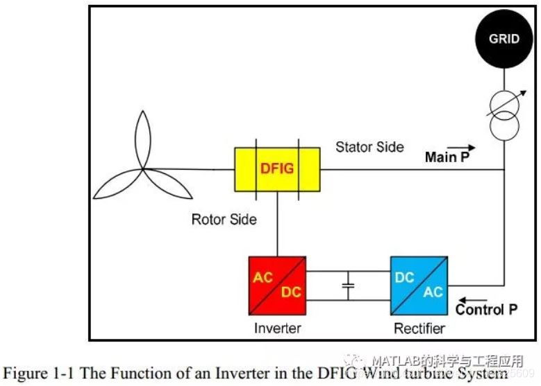
本课题研究动机是需要新设计的逆变器作为计算机与实验室级别风力涡轮机模型之间的中间设备。这种类型的风力涡轮机用于教学和培养工程师,并提取风力发电的实验数据。然而,由于商用逆变器不能够接收从计算机发送的主参考信号,以操作实验室级别的风力涡轮机,因此需要设计可控、可变的逆变器来接收该信号。
在VSI平台上搭建了电压源逆变器(VSI)和电流控制电压源逆变器(CC-VSI),在CSI平台上搭建了电流源逆变器(CSI)。此外,还设计了TMS320F2812的模拟数字转换器(ADC)驱动电路和输出LC滤波器作为辅助电路。编写了5种PWM开关程序,3种开关程序用于VSI,一种用于CC-VSI,一种用于CSI。采集了上述软硬件结合的输出波形,能够很好地跟踪主参考信号。虽然每个逆变器的性能良好,但是VSI结合空间矢量PWM开关算法能够产生具有最小噪声量的最干净的输出电压波形。
本文设计的逆变器可以应用于实验室规模的风力涡轮机、太阳能电池板的最大功率跟踪、分析数字信号处理的设备。然而,在这些应用中使用逆变器之前,要解决死区时间引起的信号失真、固定开关频率引起的谐波信号以及安装在面包板上引起的可靠性问题等许多工作。综上所述,虽然本文没有详细说明这三台逆变器的整个过程,也没有详细说明每台逆变器的构造要求,但提供了足够的逆变器拓扑、硬件设计和PWM开关算法等信息,根据这些信息完全可以重新复现三相逆变器的设计。
The goal of this thesis project was to design and build a three-phaseinverter controlled by the TMS320F2812DSP by Texas Instruments. The TMS320F2812is controlled in order to make inverters generate output waveforms which mimicthe main reference signal coming from a computer. The project included buildingthree different inverters on two platforms including auxiliary circuits anddesigning five pulse width modulation (PWM) switching algorithms for the inverters.The motivation was that a newly designed inverter was required as an intermediarydevice between a computer and a laboratory-scaled model of a wind turbine. Thistype of wind turbine is used to educate students and engineers and to extract experimentalwind power data. However, since commercial inverters don’t follow the mainreference signal which is sent from the computer in order to operate thelaboratoryscaled wind turbine, a controllable and variable inverter needed tobe designed to receive that signal. The results are as follows. The voltagesource inverter (VSI) and the currentcontrolled voltage source inverter(CC-VSI) were built on the VSI platform, and the current source inverter (CSI)was built on the CSI platform. Furthermore, the TMS320F2812’sanalog digital converter (ADC) driver circuit and the output LC filter werealso designed as auxiliary circuits. Five PWM switching programs were written; threeswitching algorithms for the VSI, and one algorithm each for the CC-VSI and theCSI. The output waveforms from the combination of hardware and softwarementioned above were captured, and they follow the main reference signal verywell. Although each of the inverters performed well, the VSI in combinationwith the Space Vector PWM switching algorithm produced the cleanest outputvoltage waveforms with the least amount of noise. The inverters built in thisthesis project can be applied to the laboratory-scaled wind turbine, themaximum power tracking in solar panels, and equipment for analyzing digitalsignal processing. However, before using the inverters in those applications,much work remains to be done to solve the problems related to the signaldistortion caused by the dead band time, harmonic signals caused by the fixedswitching frequency, and the reliability issues caused by mounting on the breadboard. In conclusion, although this thesis does not illustrate the entireprocess of or explain every requirement for building the three inverters,enough information about the topology of the inverters, the hardware design,and the PWM switching algorithms is provided in this thesis to enable one toremake all three of the three-phase inverters.
1 引言
2 逆变器理论
3 TMS320F2812的基本功能
4 TMS320F2812的具体实现
5 硬件设计与实现
6 结论与未来研究展望
下载英文原文地址:
http://page5.dfpan.com/fs/8lccdje2b2c182c9163/
更多精彩文章请关注微信号: