ADC/DAC and Digital Audio Processing
In this lab, Analog-to-Digital Converters, Digital-to-Analog Converters (DAC), sampling, and quantization basics are discussed. The ADAU1761 audio Codec chip (coder-decoder) mounted on the Zedboard is used for audio processing. The Codec is configured through I2C bus, which is also covered here in depth. An application is developed to utilize the two ADCs of the Codec to sample stereo audio (Right channel + Left channel) at 48Khz. The digitized samples are sent to the Zynq chip through the I2S standard audio bus for processing. On the Zynq chip, a dedicated hardware called NCO (Numerically Controlled Oscillator) is responsible for generating samples of sine wave at selected frequencies. These samples of sine wave is superpositioned on the received audio samples. The modified audio samples (received audio samples + sine wave samples) are sent over the I2S bus to the DAC converters of the Codec for playing on a speaker ( or an earphone) connected to the line out port of the chip. I2S standard audio bus is examined as well.

Lab 8 Design Flow

Lab8 Block Diagram

Lab8 Board Interface
Audio signals are analog signals that have to be converted to digital forms in order to be processed by an embedded system, the figure below shows an example of an audio signal.

Sample of an audio signal
Analog to digital converters (ADC) are used to digitize audio signals. According to Nyquist theorem, the sampling frequency of an audio ADC should be at least twice the highest frequency component of audio (22Khz). Therefore, the sampling frequency should be no less than 44Khz. After obtaining digitized samples of an audio signal, processing can take place in a digital system (DSP, Microprocessor, or Microcontroller), the processing performed vary in complexity depending on application. It could be as complex as voice recognition, or it could be something simpler like filtering or mixing. If it is wished to play back the processed audio, a digital to analog converter (DAC) is needed, the DAC converters the stream of digital values into an analog signal, and this newly constructed analog signal could be sent to a speaker for playing.

Typical Digital Audio Processing System
On the Zedboard, a chip named ADAU1761 Codec (coder-decoder) is dedicated for audio, it is a quite sophisticated chip equipped with two 24-bit ADCs and two 24-bit DACs with a wide range of supported sampling rate from 8Khz to 96Khz.
In this lab, the two ADCs of the Codec are configured to sample stereo analog audio (Right channel + Left channel) at 48Khz, the digitized samples are sent to the Zynq chip through the I2S standard audio bus for processing(The zed_audio_ctrl IP core by the Zynq Book Team is used to implement the I2S interface ). On the Zynq chip, A dedicated hardware called NCO (Numerically Controlled Oscillator- Credit to the Zynq Book Team) is responsible for generating samples of sine wave at selected frequencies. These samples of sine wave can be superpositioned on the received audio samples using the switches on the Zedboard. The modified audio samples (received audio samples + sine wave samples) are sent over the I2S bus to the DACs converters of the Codec for playing on a a speaker or an earphone connected to the line out port of the chip(green plug). The input analog audio could be fed from a microphone, or from an analog audio output of a desktop or a laptop(blue plug).

ADAU1761 Codec Interface
The audio cable to be used should be 2-channels (stereo) compatible.

Connection diagram for standard stereo audio cable
The frequency of the sine wave to be superpositioned on the input audio is set with respect to the eight switches available on the Zedboard. The binary value equivalent to the switches status is presented on the LEDs for the purpose of providing basic visual feedback. To use the ADAU1761 Codec, it has to be configured first. The configuration is done by sending commands over the I2C bus. This is why we need to enable the I2C controller on the PS side of the Zynq chip. The Codec requires an external clock supply, the PS’s FCLK_CLK1 is configured to provide 10Mhz clock to the Codec.
Background
A-ADAU1761 Codec
The ADAU1761 by Analog Devices is a rich audio chip that can be used for multiple acoustic purposes such as: playing, recording, processing. It has two 24-bit audio ADCs and two 24-bit DACs converters, a fully independent Sigma DSP core is available within the chip to provide autonomous operation (NOT USED IN THIS LAB), sampling rate from 8 Khz to 96Khz is supported. The sampling frequency is generated by the PLL logic which is driven by a master clock supplied by an external source(in here we supplied 10Mhz on FCLK_CLK1 of the PS ). Captured and transmitted digital audio is read/written through the data port of the chip, the data port is compliant with the I2S audio interface standard.

ADAU1761 Codec Block Diagram

ADAU1761 Codec Detailed Block Diagram
Besides the data port, the Codec has a control port. Prior of using the chip, it needs to be configured first. The configuration is achieved by sending commands through the control port which is I2C compatible. The control port essentially provides access to the chip’s control registers. There are 67 control registers, the addresses of these 67 registers are in the range of 0x4000 to 0x40FA. Writing to these registers sets different aspects of the chip, such as: controlling the internal audio amplifiers gain, enabling/disabling mixers, switching ON/OFF various parts of the chip, setting up the sampling frequency. For instance, Examine register R19 (address 0x4019), by writing the binary value ( x0000011) to that register, both ADCs in the chip are enabled.

R19 Control Register inside the ADAU1716 Codec
Taking another example, writing the binary value of 0 to register 61 (address 0x40F5) disables the DSP core within the Codec.

R61 Control Register inside the ADAU1716 Codec
B-I2C Bus
The I2C bus is used to configure the Codec by writing to its control registers. The serial data (SDA) line on the I2C bus carry configuration commands between the I2C master controller(Zynq chip) and the Codec which is synced by serial clock (SCL) line. The ADAU1761 Codec is always a slave on the bus, which means that it cannot initiate a data transfer. I2C slave devices are recognized by a unique 7-bits address. Bits[6:2] of the I2C address for the ADAU1761 are fixed to (01110)2, however, Bits[1:0] are not. In this lab they are set by the levels on the ADDR1 and ADDR0 ports defined in the system block diagram of the PS and they are both driven by logic level zero. Bits[1:0]= (00)2.Therefore, the complete address of the Codec is (0111000)2 or (0x38) in hexadecimal.
Initially, the Codec is at idle state and monitors the SDA and SCL lines for a start condition, and its specific address. The I2C master (Zynq chip) initiates a data transfer by establishing a start condition, defined by a high-to-low transition on SDA while SCL remains high. This indicates that an address/ data stream follows. The Codec shifts the next eight bits (the 7-bit address plus the R/W bit) MSB first. The Codec recognizes the transmitted address and responds (acknowledges) by pulling the data line low during the ninth clock pulse. This ninth bit is known as an acknowledge bit, by which the master knows that the Codec is up and running, and willing to cooperate. After that, the I2C master sends the sub-address high byte of the control register it wishes to write to, the Codec acknowledges the reception of the byte by pulling the data line low during the ninth clock pulse. The next byte to send is the lower sub-address byte of the control register to write to, in a similar fashion the Codec also acknowledges at the ninth clock cycle. Finally, the data to be written to the control register is sent and should be acknowledged on the ninth cycle by the Codec. This is known as a single-word write operation. Which is terminated by the master with a stop condition. The figure below shows the format of a single-word write operation. Every ninth clock pulse, the Codec issues an acknowledge by pulling SDA low. Notice that in order to write a byte to a control register using I2C , four bytes were actually sent:
1.Byte1: I2C address for the ADAU1761 (0x38).
2.Byte2: Sub-address high byte of the control register.
3.Byte3: Sub-address low byte of the control register.
4.Byte4: The data byte to be written in the control register.

Single-word I2C write operation

Single-word I2C write operation digital waveform
Going back to the DSP core disable example, The DSP core is associated with control register 61 (address 0x40F5). Four bytes need to be sent over the I2C bus to perform the switch disable command. The first byte is the chip address (0x3B), the second byte is the subaddress high byte (0x40), followed by the subaddress low byte (0xF5) , and finally the data which in this very case is (0x00).
C-I2S Bus
The I2S (Inter-IC Sound) is a de-facto standard for transferring audio data within digital systems. The signals in the I2S protocol are two clocks and data lines known as the serial audio data in/out lines:
1.The Left-Right clock (LRCLK).
2.Bit clock (BCLK).
3.Serial audio data in/out lines (SDATA_ADC) and (SDATA_DAC) .

Inter-IC Sound (I2S) Protocol
The function of the Left-Right clock (LRCLK) is to identify the audio system sample rate and frame the two channels of audio data that exist on the single audio data line. As a result of the first mentioned function, the required frequency of the Left/Right clock signal is always at the system audio sample rate, such as 44.1 kHz, 48 kHz(Used in this lab), etc. The high and low times of this clock are used to separate the Left and Right channel data. The Bit clock (BCLK) is also often referred to as the serial clock. The sole purpose of the bit clock is to time the shift of audio data bits into or out of the data audio port. The minimum required frequency for the bit clock is directly related to the system audio sample rate and the audio word length. Recall that there are two channels of audio data presented in each period of the Left/Right clock, and the frequency of the Left/Right clock must be at the audio sample rate. Therefore, the minimum required bit clock frequency is twice the audio sample rate times the number of bits in each audio word. As for the serial audio data in/out (SDATA) lines, they carry the audio data, whether it is coming out of the ADC, or sent to the DAC, this is why we have two of them in this lab.
One of the industry standards for representing audio data is a word comprised of 24-bit coded in two’s-complement fix point format. The audio data word is always transmitted with the Most Significant Bit (MSB) first. Fix point numbers are specified by an A.B notation, where A is the number of bits to the left of the decimal point and B is the number of bits to the right of the decimal point. The ADAU1761 uses two’s-complement fix point format of 1.23 for both the ADC output and the DAC input.

1.23 Fixed Point Data Format

1.23 Fixed Point Data Format Notation
D-Numerically Controlled Oscillator (NCO By the Zynq Book Team)
The NCO is used to generate a sine wave at a desired frequency (within the audible range), the NCO is implanted in hardware as an AXI core to provide accurate timing. Two driver functions are available to utilize the core:
XNco_SetStep_size_v() // Setup the frequency of the sine wave.
XNco_GetSine_sample_v() // Get the sine wave sample at the requested frequency.
Note that the sample returned by the core is format-compatible with the audio, i.e. it is also in two’s-complement 1.23 fixed-point format. Internally the core is implemented as a sine wave look up table of 4096 values of signed fixed-point representing a sine wave.

Look Up Table for a sine wave
Objectives
1.Explore the digital and analog components needed to process an analog signal such as audio.
2.Present the architecture of the ADAU1761 audio Codec.
3.Study the Inter-Integrated Circuit (I2C) interface protocol and use it to communicate with an external chip.
4.Study the Inter-IC Sound (I2S) interface protocol and utilize it to exchange audio data with an external chip.
5.Examine the formats in which audio data is stored and processed.
6.Build a simple digital audio processing application.
Procedures
A-Download zed_audio_ctrl and xilinx_com_hls_nco_1_0 IP cores from GitHub
Download the following two IP controllers from my GitHub page Here ( If you are unfamiliar with downloading files from GitHub, you can refer to Procedure A-Lab2 ). Keep in mind that these IP cores are archived in a compressed file that needs to be extracted.
1.zed_audio_ctrl IP controller responsible for exchanging data with the ADAU1761 Codec through the I2S protocol.
2.xilinx_com_hls_nco_1_0 IP controller responsible for generating sine waves at a desired frequency.
These IP controllers are developed by (Louise Crockett, Ross Elliot, Martin Enderwitz, Bob Stewart, David Northcote of the Zynq book team). Make sure to save them in a directory you can easily refer to and does not contain any spaces. Such as “C:\ip_cores“. After that, extract the IP cores in the same directory.

Extract the IP Cores
B-Create a project in Vivado to target the Zedboard
Follow the same five steps in Procedures-A of Lab1. However, in step3 name your project “lab8”.
C-Create an embedded processor project using the IP Integrator
Follow the same four steps in Procedures-B of Lab1.
D-Configure the ZYNQ7 Processing System
1.Click Run Block Automation in the green information bar. In the Run Block Automation window, leave all options as is. Click OK.

Run Block Automation-Leave default settings
The PS should look like the figure below. Note: Not all the components enabled by the default settings are needed in this lab, For example: Ethernet ,USB, and timers are not needed,but for the sake of keeping the procedures section as short as possible I kept them, you can disable them if you like.

ZYNQ7 Processing System after running Block Automation with default settings
2.Double click on the ZYNQ7 Processing System to open its Re-customize IP window. In MIO Configuration enable the I2C 1 controller.

MIO Configuration – Enable I2C 1
3.In the Clock Configuration page, expand PL Fabric Clocks, enable FCLK_CLK1 and set it to 10 Mhz.

MIO Configuration – Enable FCLK_CLK1 and set to 10Mhz
This is the clock to drive the ADAU1761 Codec. Click OK to close the Re-customize IP window. The PS should look like the figure below now:

ZYNQ7 Processing System after enable I2C 1 and FCLK_CLK1
4.Hove the mouse over IIC_1 port until it changes to a pencil shape. Right click and select Make External.

Make IIC_1 Port External
5.Repeat step4 to port FCLK_CLK1. The PS should look like this :

ZYNQ7 Processing System after making IIC_1 and FCLK_CLK1 external
E-Add the zed_audio_ctrl and xilinx_com_hls_nco_1_0 IPs to Vivado IP Repository.
In Vivado, Click on the Project Settings tab available in the Flow Navigator pane. Select IP, then click on the green + symbol in the IP Repositories sub-view. A browsing window will open up, browse to the location where you extracted the IPs “C:\ip_cores” , click Select.

Project Settings Window

Brows to the location where the IPs are saved
Now, Vivado detects the new IPs in this directory, click Apply then OK.

IP Repository after refering to the location where the IPs are saved
With this you have added the zed_audio_ctrl and xilinx_com_hls_nco_1_0 to the IP repository of the current project, the next step is to add it to the block design and connect it to the Zynq processing system.
F-Add and connect zed_audio_ctrl and NCO IPs to the design
1.In the diagram view, right-click anywhere and select Add IP![]() . Enter “nco” in the search field. Select and double click on Nco to add it.
. Enter “nco” in the search field. Select and double click on Nco to add it.

Add NCO IP Core
2.Notice that Designer Assistance is available in the upper left side of the diagram view. Click on Run Connection Automation. The Run Connection Automation window will pop up, leave all default options as is, and click OK.
3.Repeat step 1&2 for zed_audio_ctrl .
4.Right click on a free location in the diagram view and select Regenerate layout ![]() . The block diagram should be similar to the one below:
. The block diagram should be similar to the one below:

Block Diagram after adding and connecting zed_audio_ctrl and xilinx_com_hls_nco_1_0 IPs
5.Hove the mouse over BCLK port on the zed_audio_ctrl until it changes to a pencil shape. Right click and select Make External.(You can do that also by hitting the Ctrl+T keys).
6.Repeat step5 for LRCLK, SDATA_O and SDATA_I on the left side of the block. The block diagram should look like this:

Define external ports for zed_audio_ctrl
These ports are going to be associated with pins connected to the ADAU1761 audio Codec, namely the left-right clock (LRCLK), bit clock (BCLK) and serial audio data in/out lines (SDATA_I=SDATA_ADC) and (SDATA_DAC=SDATA_O) .
G-Add GPIO IP core in dual channels mode
1.Click on the Add IP![]() button. From the IP catalog, double-click AXI GPIO to add it.You can type the name ” gpio” in the search field.
button. From the IP catalog, double-click AXI GPIO to add it.You can type the name ” gpio” in the search field.

Add GPIO
2.The GPIO is going to be configured to have two channels, one for LEDs and one for switches. This alternative is less area consuming than using two separate GPIOs(Done in Lab1). Double click on the GPIO block to open its Re-customize IP window. In the Board tab, set IP interface GPIO (channel 1) to leds_8bits, and GPIO2 ( channel 2 ) to sws_8bits as shown in the figure below. Click OK to exit the Re-customize IP window.

Configure dual channels GPIO
3.Notice that Designer Assistance is available in the upper left side of the diagram viewer, Click on Run Connection Automation, and select All Automation(3 out of 3 selected). to connected the IP core to the PS internally and to LEDs and switches externally. Click OK.

Run Connection Automation- GPIO dual channels

Create Port
H-Assign values to the lower bits[1:0] of ADAU1761 I2C address
1.Right click on an empty space in the diagram view, and select Create Port.
2.In the Create Port window, enter parameters as in the figure below.

Create Port Window
3.In the diagram view, right-click anywhere and select Add IP![]() . Enter “cons” in the search field. Select and double click on Constant to add it.The constant IP core is used to tie port “ADDRESS[1:0]” to a fixed logical value of zero.
. Enter “cons” in the search field. Select and double click on Constant to add it.The constant IP core is used to tie port “ADDRESS[1:0]” to a fixed logical value of zero.

Constant IP core
4.Double click on the Constant IP core to open its Re-customize IP window, set the parameters as specified in the figure below:

Constant IP core configuration
5.Connect Constant port “dout[1:0] “ to port “Address[1:0]” using the mouse.
6.Right click on a free location in the diagram view and select Regenerate layout ![]() . Your block diagram should be similar to the one below:
. Your block diagram should be similar to the one below:

Block Diagram after adding all needed IP cores for lab8
I-Add physical constraints
1.In the Flow Navigator window, select Add Sources from the Project Manager section.

Add Sources
2.The Add Sources dialogue will open. Select Add or Create Constraints.

Add or Create constraints
3.Click Next, then click on the green + symbol and select Create File

Create a new constraint file
In the next window, Select XDC as the File type and enter adc_dac_audio as the File name

Name new constraints file: adc_dac_audio
Click OK, then click Finish in the next window to create the file and close the dialogue.
In the Sources tab, expand the Constraints group and open the newly created XDC file by double clicking on adc_dac_audio.xdc

Sources pane with adc_dac_audio selected
Add the following lines to the constraints file, alternatively, it can be copied from the constraints file adc_dac_audio.xdc available on a my GitHub page.
# ZedBoard Audio Codec Constraints
set_property PACKAGE_PIN AA6 [get_ports BCLK]
set_property IOSTANDARD LVCMOS33 [get_ports BCLK]set_property PACKAGE_PIN Y6 [get_ports LRCLK]
set_property IOSTANDARD LVCMOS33 [get_ports LRCLK]set_property PACKAGE_PIN AA7 [get_ports SDATA_I]
set_property IOSTANDARD LVCMOS33 [get_ports SDATA_I]set_property PACKAGE_PIN Y8 [get_ports SDATA_O]
set_property IOSTANDARD LVCMOS33 [get_ports SDATA_O]#MCLK
set_property PACKAGE_PIN AB2 [get_ports FCLK_CLK1]
set_property IOSTANDARD LVCMOS33 [get_ports FCLK_CLK1]set_property PACKAGE_PIN AB4 [get_ports iic_1_scl_io]
set_property IOSTANDARD LVCMOS33 [get_ports iic_1_scl_io]set_property PACKAGE_PIN AB5 [get_ports iic_1_sda_io]
set_property IOSTANDARD LVCMOS33 [get_ports iic_1_sda_io]set_property PACKAGE_PIN AB1 [get_ports {ADDRESS[0]}]
set_property IOSTANDARD LVCMOS33 [get_ports {ADDRESS[0]}]set_property PACKAGE_PIN Y5 [get_ports {ADDRESS[1]}]
set_property IOSTANDARD LVCMOS33 [get_ports {ADDRESS[1]}]
Click Save ![]() . The physical constraints here connect: BCLK, LRCLK, SDATA_O, SDATA_I, FCLK_CLK1, iic_1_scl_io, iic_1_sda_io, ADDRESS[0], and ADDRESS[1] ports in the block diagram design to the actual physical pins connected to the ADAU1761 audio Codec.
. The physical constraints here connect: BCLK, LRCLK, SDATA_O, SDATA_I, FCLK_CLK1, iic_1_scl_io, iic_1_sda_io, ADDRESS[0], and ADDRESS[1] ports in the block diagram design to the actual physical pins connected to the ADAU1761 audio Codec.
J-Generate Bitstream
1.In the Sources pane, Right click on system.bd and select Create HDL Wrapper to create the top level Verilog file from the block diagram. Select Let Vivado manage wrapper and auto-update when prompted with the next message. Notice that system_wrapper.v got created and placed at the top of the design sources hierarchy.

Create HDL Wrapper
2.In the Program and Debug section in the Flow Navigator pane, click Generate Bitstream. A dialog box will appear to ask you to save the modification you made, click Save .

Generating Bitstream
Generating the Bitstream may take a while to complete, depending on the performance of your machine. After the bitstream generation completes select View Reports in the dialog box, and click OK.
K-Export hardware design to SDK
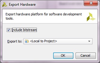
1.Click File > Export > Export Hardware, make sure you select Include bitstream.
Export Hardware to SDK
2.Select File>Launch SDK. This will open up SDK, notice that all the files related to design including the IPs has now been exported to SDK.
L-Working with SDK
1.In SDK, select File > New > Application Project.
2.In the next window, enter the parameters as provided in the snapshot below:

New Standalone C Project – audio_test
In the next window, select Empty Application from the available templates and click Finish. This will compile the BSP and the related drivers.
3.Expand audio_test project directory, right click on src directory, New->Source File.

New C Source File – lab8.c
4.In the next window that shows up type “lab8.c” in the source file and click Finish. This will create an empty C file in the src directory.

lab8.c empty source file created in SDK
5.Expand audio_test project directory again , right click on src directory, New->Header File.
6.In the next window that shows up type “audio.h” in the header file and click Finish. This will create an empty header file in the src directory.

audio.h empty header file created in SDK
7.Paste the content of lab8.c ( Available on my Github page) in in the editor view of lab8.c of SDK , similarly , paste the content of header file audio.h ( Available on my Github page) in the editor view of audio.h of SDK. Click on Save ![]() or hit (Ctrl+S) , by doing so both lab8 application, and its BSP are compiled automatically and the executable .elf file is generated( the default settings of SDK triggers compilation with Save). This is the executable file that the ARM processor on the PS side of the Zynq will execute.
or hit (Ctrl+S) , by doing so both lab8 application, and its BSP are compiled automatically and the executable .elf file is generated( the default settings of SDK triggers compilation with Save). This is the executable file that the ARM processor on the PS side of the Zynq will execute.
M-Download bitstream and run the application (Hardware Verification)
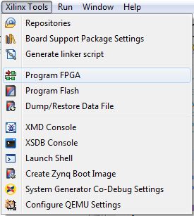
1.Select Xilinx Tools-> Program FPGA to download the Bitstream (this will take few seconds).
Downloading Bitstream to the PL
2.Select audio_test project directory-> Run As-> Launch on Hardware (GDB) to run audio_test application on the ARM processor.

Run application on ARM processor
After download is complete, connect a speaker or an earphone to the Line out (green plug), turn ON and OFF different switches on the board to hear different tones ( sine waves at different audible frequencies). Connect the Line in (blue plug) to the output headset port of your laptop or desktop using a 3.5mm jack male-to-male-stereo cable.

3.5mm jack male-to-male-stereo cable
An audio will be heard on the speaker, which you can mix sine waves with it using the switches on the Zedboard. What is actually happening behind the scenes, the ADAU1761 Codec is converting the analog audio coming from the your workstation into digital audio data that is sent to the Zynq chip through the I2S bus. The Zynq chip has full access to the audio data and can do any kind of digital signals processing( In here we are just adding sine wave) the modified audio data is sent back to the ADAU1761 through the I2S bus. The DAC converter on the ADAU1761 Codec is responsible for constructing a new analog audio signal that includes the original audio plus the sine waves superimpositioned on top of it. The DAC output is connected to the speaker (or earphone). See demo video :
By this you have completed Lab8-ADC/DAC and Digital Audio Processing. You can find the complete solution of this lab in here.