在用ISE设计FPGA电路时,对Verilog HDL语言描述的电路经过综合,得到两种不同的原理图表现形式:

由ISE的界面,可见分别为:RTL Schematic与Technology Schematic,这两者到底由什么区别呢?
在我的博文中,凡是用Verilog HDL描述的电路,一般我都会放上这两个原理图。例如:
来个简单的示例吧:通过仿真和综合认识T触发器(Verilog HDL语言描述T触发器)
这篇博文中,我通过综合得到了的RTL Schematic如下:
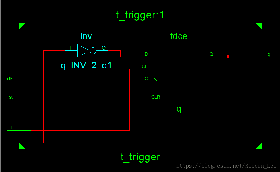
从这张图中我们可以清晰的看出T触发器是一些门级元件构成,分别为反相器(非门)和D触发器。
再看Technology Schematic
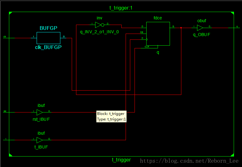
可见,这个电路是由全局时钟缓冲器(BUFGP)以及各种输入输出缓冲(ibuf)(obuf)以及非门、D触发器组成,这些东西都是FPGA底层的元件,FPGA内部就是由这写东西来组成一系列的电路的,所以这说明了什么呢?
说明了Technology Schematic,这种原理图是FPGA实际的电路图样子,是在FPGA中综合的效果。
相反,RTL Schematic是语法分析得到的结果,类似于你用原理图设计电路的样子。
下面内容来自于:RTL 与 technology schematic的区别,包含概念与实例
http://china.xilinx.com/support/answers/41500.html#solution
下面选自网上的一些说法,仅供参考:
rtl视图,其实就是寄存器级传输图,它在综合及布局布线前就生成了,并非设计的最终电路结构,是设计输入的最忠实的体现,它的主要作用是帮助设计者检查设计输入中的问题。就像是用XST综合的时候,有一个view rtl schematic和一个view technology schematic,区别是前者仅仅是语法分析得到的结构,是你的设计单纯的综合效果,可以帮助你理解你的算法;而后者才是放在FPGA中综合的效果,是用chipscope可以看到的,反映了实际的电路和资源使用情况。
RTL View
Viewing an RTL schematic opens an NGR file that can be viewed as a gate-level schematic.
This schematic is generated after the HDL synthesis phase of the synthesis process. It shows a representation of the pre-optimized design in terms of generic symbols, such as adders, multipliers, counters, AND gates, and OR gates, that are independent of the targeted Xilinx device.
查看RTL schematic,将会打开NGR文件,该文件被看做门级的schematic。RTL schematic在synthesis过程的HDL synthesis phase之后产生,他是用通用的symbol表征的优化前的设计,比如 adders, multipliers, counters, AND gates, and OR gates,与目标器件是独立的。
Technology View
Viewing a Technology schematic opens an NGC file that can be viewed as an architecture-specific schematic.
This schematic is generated after the optimization and technology targeting phase of the synthesis process. It shows a representation of the design in terms of logic elements optimized to the target Xilinx device or "technology"; for example, in terms of of LUTs, carry logic, I/O buffers, and other technology-specific components. Viewing this schematic allows you to see a technology-level representation of your HDL optimized for a specific Xilinx architecture, which might help you discover design issues early in the design process.
You should always refer to technology schematic for synthesized result.
To disable RTL schematic generation to speed up synthesis, you can set XST property Generate RTL Schematic (-rtlview) to "No".
查看RTL schematic,将会打开NGC文件,该文件被看做基于结构的schematic。
该schematic在synthesis过程的optimization and technology targeting phase之后产生,该schematic示的是根据 Xilinx的device or "technology优化之后,用logic elements组成的schematic。例如,用 LUTs, carry logic, I/O buffers, and other technology-specific components。查看该schematic,可以看到杜宇一个特定的xilinx器件结构优化之后的technology-level的表示,这将帮助你在设计过程中尽早发现设计问题。
RTL的一种翻译是寄存器传输级的电路,参考:寄存器传输级,这篇文章可以帮助理解什么是寄存器传输级。