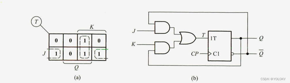
5-7题目更正:为了确定驱动JK触发器J端和K端的组合逻辑,应列出JK触发器的特性表,并在该表右侧逐行列出对T触发器的驱动要求,即T端所要求的逻辑值。如果到
状态不变,则T=0;如果
到
状态翻转,则T=1。

-
Chapter 5
-
Chapter 5, Problem 1P
Step-by-step solution
Step 1/4
The data and clock input timing diagram is shown in Figure 1.
-
5-7题目更正:为了确定驱动JK触发器J端和K端的组合逻辑,应列出JK触发器的特性表,并在该表右侧逐行列出对T触发器的驱动要求,即T端所要求的逻辑值。如果到
状态不变,则T=0;如果
到
状态翻转,则T=1。
Chapter 5
Chapter 5, Problem 1P
Step 1/4
The data and clock input timing diagram is shown in Figure 1.