前言
(1)ARTS 挑战打卡的第3天,分享一个外网技术文章。(注:本人基本没看懂,苦笑)
(2)原文链接:https://www.embedded.com/boost-adc-throughput-by-optimizing-your-mcu-spi-driver/
Boost ADC throughput by optimizing your MCU SPI driver(通过优化 MCU SPI 驱动程序提高 ADC 吞吐量)
introduction(导言)
With the advancement of technology, the transmission of more precise data is needed in low power Internet of Things (IoT) and edge/cloud computing. In Figure 1, the wireless sensing system is a high precision data acquisition system with a 24-bit analog-to-digital converter (ADC). In this case, whether the microcontroller unit (MCU) can afford the serial high speed interface of the data converter is our problem.
随着技术的进步,低功耗物联网(IoT)和边缘/云计算需要传输更精确的数据。在图1中,无线传感系统是一个带有24位模数转换器(ADC)的高精度数据采集系统。在这种情况下,微控制器单元(MCU)能否负担得起数据转换器的串行高速接口是我们的问题。
This article describes the process of designing a high speed Serial Peripheral Interface (SPI) data transaction driver between the MCU and ADC. The following sections will show a brief description of different ways to optimize the SPI driver and the required configuration on the ADC and MCU. A detailed description of the example code of the SPI and direct memory access (DMA) data transaction will be provided after the brief illustration. Finally, a demonstration of the throughput of ADC with the same driver in a different MCU (ADuCM4050,MAX32660) will be included.
本文介绍了设计 MCU 和 ADC 之间的高速串行外设接口 (SPI) 数据事务驱动程序的过程。以下部分将简要描述优化 SPI 驱动程序的不同方法以及 ADC 和 MCU 上所需的配置。在简要说明之后将提供 SPI 和直接存储器存取 (DMA) 数据事务的示例代码的详细描述。最后,还将演示在不同 MCU(ADuCM4050、MAX32660)中使用相同驱动器的 ADC 吞吐量。
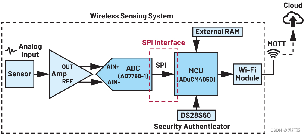
Figure 1. Condition-based monitoring.
图 1. 基于状态的监控。
Introduction to General SPI Driver(通用SPI驱动简介)
As the name suggests, MCU vendors provide general SPI driver/API in example code to each MCU. The general SPI driver/API usually can cover most users’ applications that may conclude many configurations or determine statements. In some specific scenarios, such as ADC data acquisition, the general SPI driver cannot satisfy the full speed throughput of the ADC data because too many different configurations in the general driver are implemented. The configurations that are not used in the application create additional overhead and cause a time delay.
顾名思义,MCU 供应商以示例代码的形式向每个 MCU 提供通用 SPI 驱动程序/API。通用的SPI驱动程序/API通常可以覆盖大多数用户的应用程序,这些应用程序可能会完成许多配置或确定语句。在一些特定场景下,例如ADC数据采集,通用SPI驱动程序无法满足ADC数据的全速吞吐量,因为通用驱动程序中实现了太多不同的配置。应用程序中未使用的配置会产生额外的开销并导致时间延迟。
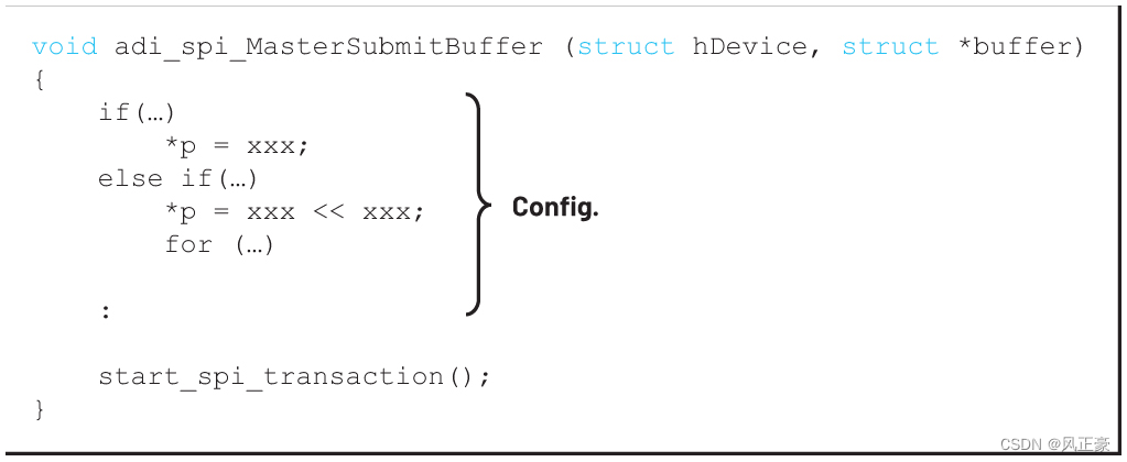

Figure 2. Configuration of a general API.
图 2. 通用 API 的配置。
Framework(框架)
To extract the output data of an ADC through SPI, we would choose an MCU as the main device for its low power consumption and high speed performance. However, when a data transaction is based on the ADI SPI driver, the speed can degrade due to commands that are not functional in the ADC-to-MCU application. To fully unleash the potential speed of the ADC, we experiment with the ADuCM4050 and AD7768-1 and try out possible solutions. Despite the maximum output data rate of 256 kHz (under the default filter), the ADuCM4050 is currently limited to 8 kHz. Potential solutions for the acceleration of the output rate include removing unnecessary commands and activation of the DMA controller. These ideas are realized in the following sections.
为了通过SPI提取ADC的输出数据,我们会选择MCU作为主要器件,因为它具有低功耗和高速性能。然而,当数据事务基于 ADI SPI 驱动程序时,速度可能会由于 ADC 至 MCU 应用中不起作用的命令而降低。为了充分发挥 ADC 的潜在速度,我们对 ADuCM4050 和 AD7768-1 进行了实验,并尝试了可能的解决方案。尽管 ADuCM4050 的最大输出数据速率为 256 kHz(在默认滤波器下),但目前仅限于 8 kHz。加速输出速率的潜在解决方案包括删除不必要的命令和激活 DMA 控制器。这些想法将在以下部分中实现。
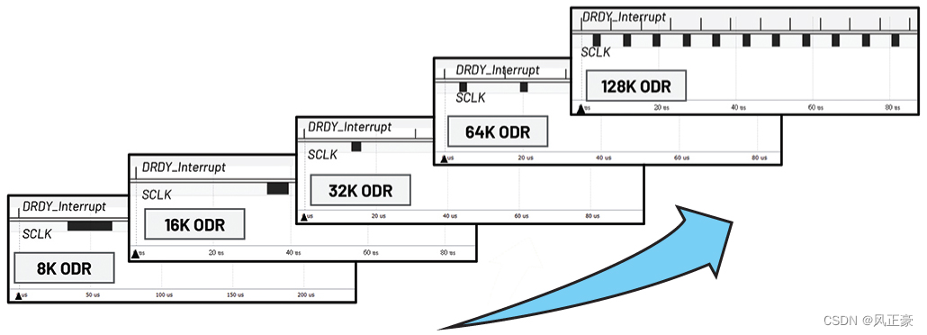
Figure 3. Different ODRs and the relationship between DRDY and SCLK.
图 3. 不同的 ODR 以及 DRDY 和 SCLK 之间的关系。
MCU as Main(MCU为主)
The ADuCM4050 MCU is an ultra low power microcontroller system with a 26 MHz main clock rate. The system is driven by the Arm® Cortex®-M4F processor. The ADuCM4050 is equipped with three SPIs, and each SPI incorporates two DMA channels, receive and transmit, that interface with the DMA controller. The DMA controller and DMA channels provide a means to transfer data between memory and peripherals. This is an efficient way to distribute data freeing up the core to handle other tasks.
ADuCM4050 MCU 是一款超低功耗微控制器系统,主时钟速率为 26 MHz。该系统由 Arm ® Cortex ® -M4F 处理器驱动。 ADuCM4050 配备三个 SPI,每个 SPI 包含两个 DMA 通道(接收和发送),用于与 DMA 控制器连接。 DMA 控制器和 DMA 通道提供了在内存和外设之间传输数据的方法。这是一种有效的数据分配方式,可以释放核心来处理其他任务。
ADC as Node(ADC 作为节点)
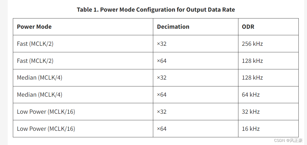
The AD7768-1 is a 24-bit, low power, high performance, sigma-delta (Σ-Δ) ADC. The output data rate (ODR) and power dissipation mode are adjustable to meet the users’ requirements. The decimation factor and power mode together determine the ODR as shown in Table 1.
AD7768-1 是一款 24 位、低功耗、高性能 Σ-Δ (Σ-Δ) ADC。输出数据速率(ODR)和功耗模式可调,以满足用户的要求。抽取因子和功耗模式共同决定 ODR,如表 1 所示。
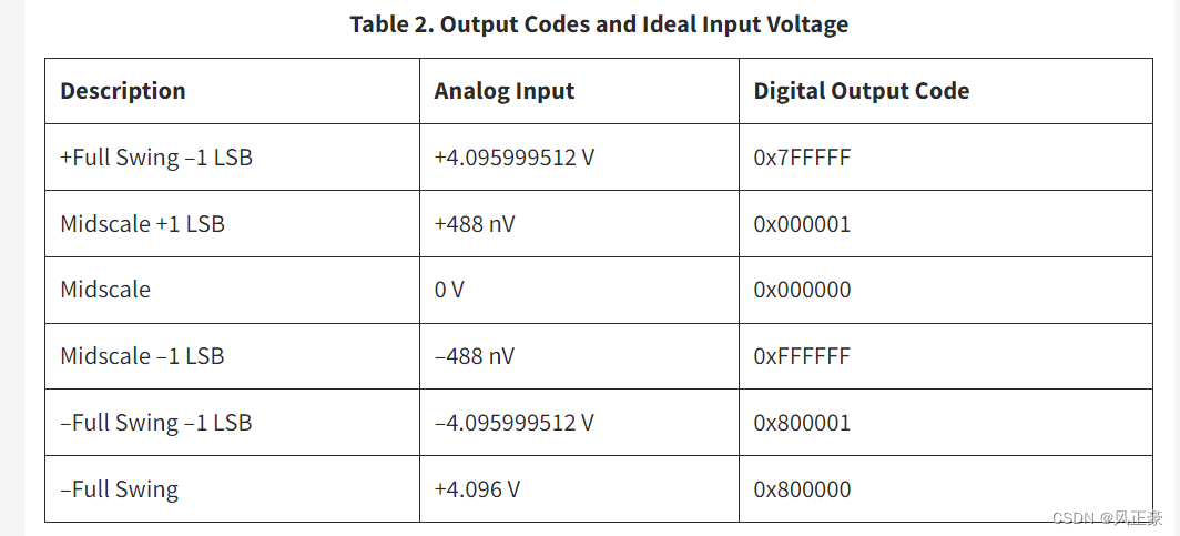
The AD7768-1’s continuous read mode is also a significant feature. The output data of the ADC is stored in the register 0x6C. In general, the data in ADC register requires address specification before each read/write operation. Continuous read mode enables direct derivation of data from the 0x6C register after each data ready signal. The ADC output data is a 24-bit digital signal that converts to volts as shown in Table 2.
AD7768-1 的连续读取模式也是一个重要特性。 ADC的输出数据存储在寄存器0x6C中。一般来说,ADC寄存器中的数据在每次读/写操作之前都需要指定地址。连续读取模式允许在每个数据就绪信号后直接从 0x6C 寄存器获取数据。 ADC 输出数据是 24 位数字信号,可转换为电压,如表 2 所示。
Connection Diagram of Data Flow(数据流连接图)
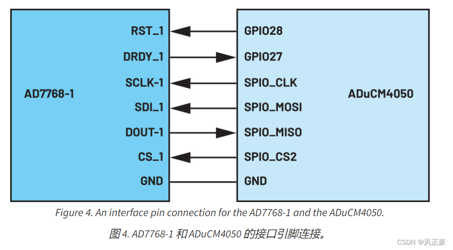
The ADuCM4050 and AD7768-1 are used as the data transaction example models. The pin connection is shown in Figure 4.
ADuCM4050 和 AD7768-1 用作数据事务示例模型。引脚连接如图4所示。
Their reset signal is sent from the MCU GPIO28 to the ADC RST_1 pin, and the data ready signal is sent from the ADC DRDY_1 to the MCU GPIO27. The rest of the pins are connected as a general SPI configuration, where the MCU is the main and ADC is the node. SDI_1 receives the ADC register read/write commands from the MCU, and DOUT_1 sends the output data to the MCU.
它们的复位信号从 MCU GPIO28 发送到 ADC RST_1 引脚,数据就绪信号从 ADC DRDY_1 发送到 MCU GPIO27。其余引脚连接为通用 SPI 配置,其中 MCU 为主,ADC 为节点。 SDI_1接收来自MCU的ADC寄存器读/写命令,DOUT_1将输出数据发送到MCU。
Realization of Data Transaction(数据交易的实现)
Interrupt Data Transaction(中断数据事务)
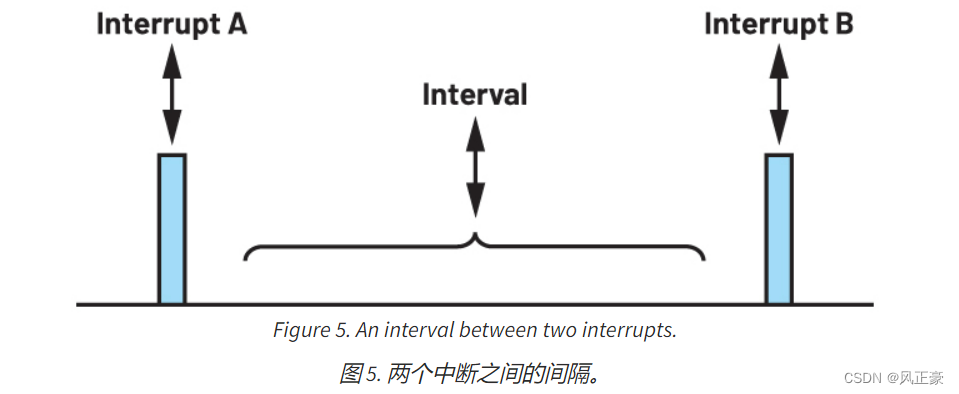
To realize the continuous data transaction, we use the GPIO27 (connected to DRDY) as the interrupt trigger. When the ADC sends a data ready signal to the GPIO27, the MCU runs the callback function, where data transaction commands are included. As shown in Figure 5, data acquisition must be handled in the interval between Interrupt A and Interrupt B.
为了实现连续数据传输,我们使用 GPIO27(连接到 DRDY)作为中断触发器。当 ADC 向 GPIO27 发送数据就绪信号时,MCU 运行回调函数,其中包含数据事务命令。如图5所示,数据采集必须在中断A和中断B之间的时间间隔内进行。
With the ADI SPI driver, we can easily realize the data transaction between the ADC and MCU. However, the ADC ODR would be limited to 8 kHz due to redundant commands in the driver. To speed up the process, we trim the codes to the slimmest. We introduce two methods for DMA data transactions: basic mode DMA transaction and ping-pong mode DMA transaction.
借助ADI SPI驱动程序,我们可以轻松实现ADC和MCU之间的数据交互。然而,由于驱动器中的冗余命令,ADC ODR 将被限制为 8 kHz。为了加快这个过程,我们将代码修剪到最精简。我们介绍两种 DMA 数据传输方法:基本模式 DMA 传输和乒乓模式 DMA 传输。
Basic Mode DMA Transaction(基本模式 DMA 事务)
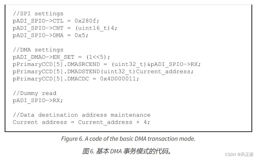
Before each DMA transaction, some SPI and DMA settings are required (see the example code in Figure 6). SPI_CTL is the SPI configuration. SPI_ CTL=0x280f is derived from the value set for the ADI SPI driver. SPI_CNT is the transfer byte count. Since each DMA transaction can only transmit a fixed bit number of 16, SPI_CNT must be a multiple of 2. In our case, SPI_CNT=4 is chosen to cover the 24-bit output data of ADC. SPI_DMA register is the SPI DMA enable. SPI_DMA=0x5 enables the receive DMA request. pADI_DMA0->EN_SET=(1<<5) enables the DMA of the fifth DMA channel – SPI0 RX.
在每个 DMA 事务之前,需要进行一些 SPI 和 DMA 设置(请参见图 6 中的示例代码)。 SPI_CTL 是 SPI 配置。 SPI_ CTL=0x280f 源自为 ADI SPI 驱动程序设置的值。 SPI_CNT 是传输字节数。由于每个 DMA 事务只能传输固定位数 16,因此 SPI_CNT 必须是 2 的倍数。在我们的示例中,选择 SPI_CNT=4 以覆盖 ADC 的 24 位输出数据。 SPI_DMA寄存器是SPI DMA使能。 SPI_DMA=0x5 使能接收 DMA 请求。 pADI_DMA0->EN_SET=(1<<5) 使能第五个 DMA 通道 – SPI0 RX 的 DMA。
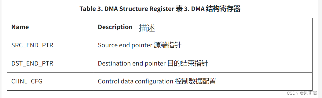
Each DMA channel has a DMA structure register shown in Table 3. Note that the end of the source address here (that is, SPI0 Rx) needs no increments during the entire operation since the Rx FIFO pushes the data out of the register automatically. On the other hand, the end of the destination address is calculated by the function (destination address + SPI_CNT -2) according to the ADI SPI driver.
每个 DMA 通道都有一个 DMA 结构寄存器,如表 3 所示。请注意,这里源地址的末尾(即 SPI0 Rx)在整个操作过程中不需要增量,因为 Rx FIFO 自动将数据从寄存器中推出。另一方面,目标地址的末尾是根据ADI SPI驱动程序通过函数(目标地址+SPI_CNT -2)计算的。
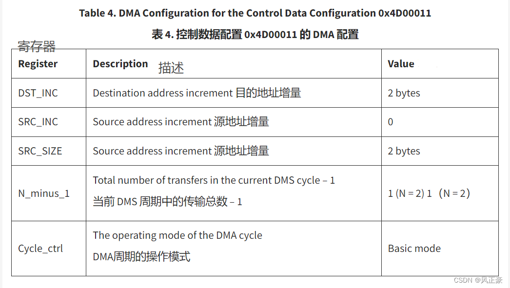
The current address here is the address of an internal array buffer. DMA control data configuration includes the settings of source data size, source address increment, destination address increment, the number of transfers left, and DMA control mode. The value 0x4D000011 sets the configuration as described in Table 4.
这里的当前地址是内部数组缓冲区的地址。 DMA 控制数据配置包括源数据大小、源地址增量、目标地址增量、剩余传输数和 DMA 控制模式的设置。值 0x4D000011 设置配置,如表 4 中所述。
With the dummy read command SPI_SPI0 -> RX, SCLK clocking starts, and the output data is transmitted from ADC to MCU through the MISO line. There are also some negligible data transfers on the MOSI line. Once the Rx FIFO is filled, the DMA request is generated, thus activating the DMA controller to transfer the data from the DMA source (that is, SPI0 Rx FIFO) to the DMA destination (that is, the internal array buffer). It is worthy of note that the Tc request is generated at SPI_DMA=0x3.
随着虚拟读命令 SPI_SPI0 -> RX,SCLK 时钟开始,输出数据通过 MISO 线从 ADC 传输到 MCU。 MOSI 线上还有一些可以忽略不计的数据传输。一旦 Rx FIFO 填满,就会生成 DMA 请求,从而激活 DMA 控制器将数据从 DMA 源(即 SPI0 Rx FIFO)传输到 DMA 目标(即内部阵列缓冲区)。值得注意的是,Tc 请求是在 SPI_DMA=0x3 时生成的。
At last, we maintain the destination address for the next 4-byte transmission by adding 4 to the current destination address.
最后,我们通过在当前目标地址上加 4 来维护下一个 4 字节传输的目标地址。
Please also be aware that both pADI_DMA0->DSTADDR_CLR and pADI_DMA0->RMSK_CLR for SPI0 DMA channel must be set in the main function before the first interrupt occurs. The prior register is DMA Channel Destination Address Decrement Enable Clear, which sets the destination address shifting after each DMA transfer in increment mode (only in increment mode does the function for destination address calculation works). The latter register is DMA Channel Request Mask Clear, which clears the DMA request status for the channel.
还请注意,SPI0 DMA 通道的 pADI_DMA0->DSTADDR_CLR 和 pADI_DMA0- SPI0 DMA 通道的 >RMSK_CLR 必须在第一次中断发生前在主函数中设置。前一个寄存器是 DMA 通道目标地址递减使能清除寄存器(DMA Channel Destination Address Decrement Enable Clear),用于设置增量模式下每次 DMA 传输后的目标地址移位(只有在增量模式下,目标地址计算功能才起作用)。后一个寄存器是 DMA 通道请求屏蔽清除寄存器,用于清除通道的 DMA 请求状态。
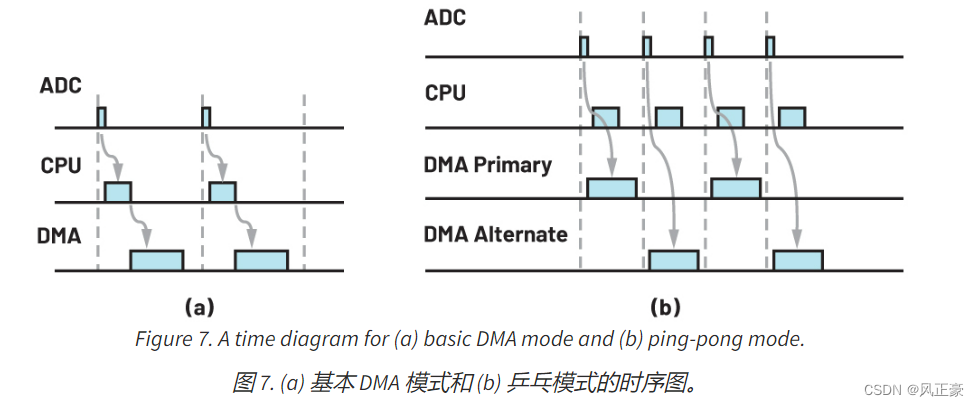
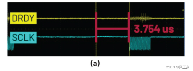
A time diagram for the basic mode DMA transaction is depicted in Figure 7a. The time slots represent the DRDY signal, SPI/DMA settings, and DMA data transaction, respectively. To better utilize the idle time of the CPU, we wish to assign tasks for the CPU while the DMA controller is handling the data transfer.
图 7a 描述了基本模式 DMA 事务的时序图。时隙分别代表 DRDY 信号、SPI/DMA 设置和 DMA 数据事务。为了更好地利用CPU的空闲时间,我们希望在DMA控制器处理数据传输时为CPU分配任务。
Ping-Pong Mode DMA Transaction(乒乓模式 DMA 事务)
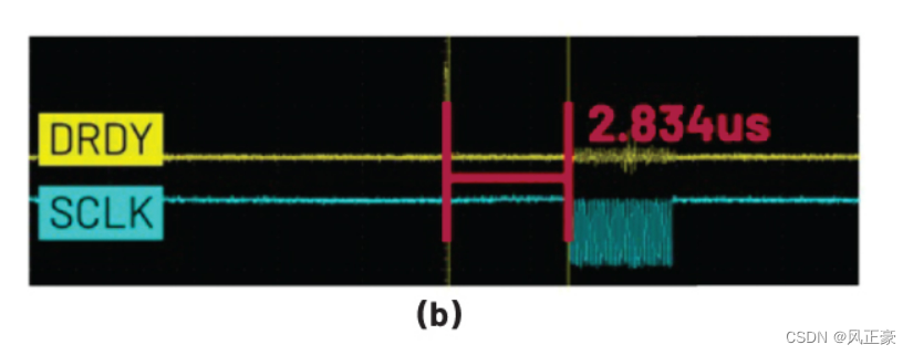
After the dummy read command is implemented, the DMA controller starts the data transaction, leaving the CPU of the MCU idle with no tasks. If we can have the CPU and DMA controller work simultaneously, the task handling is no longer serial but parallel. Therefore, we can conduct the DMA configuration (by the CPU) and the DMA data transaction (by the DMA controller) at the same time. To realize this idea, the so-called ping-pong mode is required for the DMA controller. Ping-pong mode incorporates two sets of DMA structures—primary and alternate. The DMA controller switches automatically between the two structures at each DMA request. Initially set to 0, variable p marks if the primary (p = 0) or alternate (p = 1) DMA structure is in charge. If p = 0, DMA primary data transaction starts on the dummy read command. At the same time, we assign values for the alternate DMA structure, which will be in charge in the next interrupt cycle. If p = 1, the primary and alternate structures switch their roles. The modification of the DMA structure during a DMA transaction can fail with only the primary one in basic DMA mode. The use of ping-pong mode enables the CPU to access and write the alternate DMA structure while the primary is read by the DMA controller and vice versa. As shown in Figure 7b, the DMA data transaction can be performed soon after the DRDY signal got transmitted from the ADC to the MCU since the DMA structure configuration is done in the last cycle. The CPU and DMA are now working simultaneously without one waiting for the other. We expect that there is now room for the ADC ODR up-tuning because the total operation time is significantly shortened.
执行虚拟读命令后,DMA 控制器开始数据事务,使 MCU 的 CPU 空闲,没有任务。如果我们能让CPU和DMA控制器同时工作,任务处理就不再是串行而是并行。因此,我们可以同时进行DMA配置(由CPU)和DMA数据事务(由DMA控制器)。为了实现这个想法,DMA 控制器需要所谓的乒乓模式。乒乓模式包含两组 DMA 结构——主结构和备用结构。 DMA 控制器在每次 DMA 请求时自动在两种结构之间切换。变量 p 最初设置为 0,标记主要 (p = 0) 还是备用 (p = 1) DMA 结构负责。如果 p = 0,则 DMA 主数据事务在虚拟读命令上启动。同时,我们为备用 DMA 结构分配值,该结构将在下一个中断周期负责。如果 p = 1,则主要结构和替代结构交换其角色。在 DMA 事务期间对 DMA 结构的修改可能会失败,仅在基本 DMA 模式下进行主要修改。使用乒乓模式使 CPU 能够访问和写入备用 DMA 结构,同时 DMA 控制器读取主结构,反之亦然。如图 7b 所示,由于 DMA 结构配置是在最后一个周期完成的,因此 DRDY 信号从 ADC 传输到 MCU 后不久就可以执行 DMA 数据事务。 CPU 和 DMA 现在同时工作,无需等待另一方。我们预计 ADC ODR 现在还有调整的空间,因为总操作时间显着缩短。
Interrupt Handler Optimization(中断处理程序优化)
The time interval between the data ready signal does not only include the conduct time of the commands in the callback function but also the ones in the ADI GPIO interrupt handler.
数据就绪信号之间的时间间隔不仅包括回调函数中命令的执行时间,还包括 ADI GPIO 中断处理程序中命令的执行时间。
At the activation of the MCU, the CPU runs the start-up file (that is, startup.s). All the event handlers are defined in the file, including the GPIO interrupt handler. Once the GPIO interrupt is triggered, the interrupt handler function (that is, GPIO_A_INT_HANDLER and GPIO_B_INT_HANDLER in the ADI GPIO driver) is performed. In general interrupt handler functions, the CPU searches through all GPIO pins for the one that triggers, clears its interrupt status, and runs the registered callback function. In the ADC-MCU application used, DRDY is the only interrupt signal. We would thus like to trim the function to speed up the process. Possible solutions include (1) retargeting in the start-up file and (2) the modification of the original interrupt handler. Retargeting means to self-define an interrupt handler and to replace the original one in the start-up file.
MCU 激活时,CPU 运行启动文件(即startup.s)。所有事件处理程序都在该文件中定义,包括 GPIO 中断处理程序。一旦触发GPIO中断,就会执行中断处理函数(即ADI GPIO驱动程序中的GPIO_A_INT_HANDLER和GPIO_B_INT_HANDLER)。在一般的中断处理函数中,CPU 会在所有 GPIO 引脚中搜索触发的引脚,清除其中断状态,并运行注册的回调函数。在所使用的ADC-MCU应用中,DRDY是唯一的中断信号。因此,我们希望修剪该函数以加快该过程。可能的解决方案包括(1)在启动文件中重定向以及(2)修改原始中断处理程序。重定向是指自定义一个中断处理程序并替换启动文件中的原始中断处理程序。
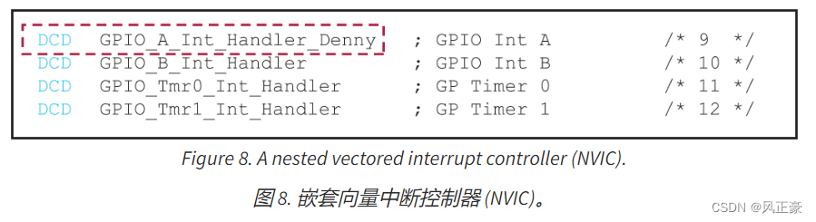
Modification, on the other hand, requires a self-defined GPIO driver. We take the latter option and modify the function as in Figure 8, where it clears only the interrupt status of the pin connected to the DRDY and goes directly to the callback function. Please note that the original GPIO driver needs to be blocked by unchecking the box of include in build target.
另一方面,修改需要自定义GPIO驱动。我们采用后一种选项并修改该函数,如图 8 所示,其中它仅清除连接到 DRDY 的引脚的中断状态并直接进入回调函数。请注意,需要通过取消选中包含在构建目标中的框来阻止原始 GPIO 驱动程序。
Result(结果)
Speed Performance(速度性能)
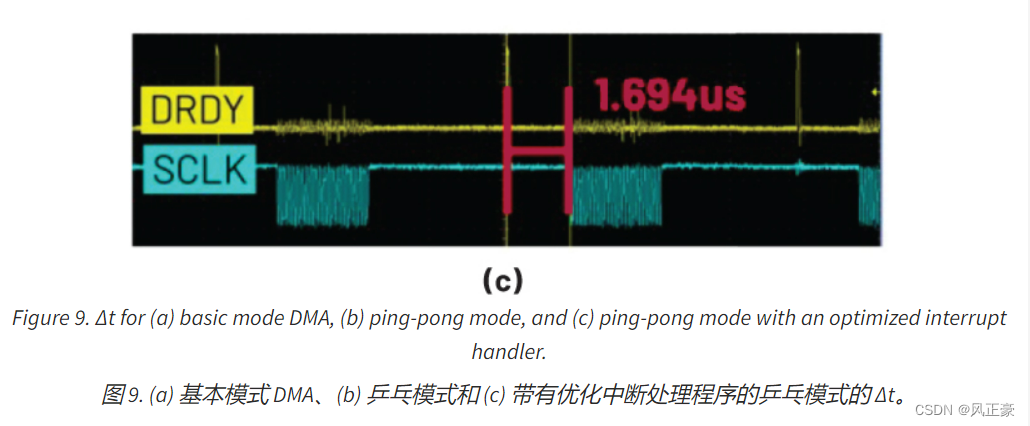
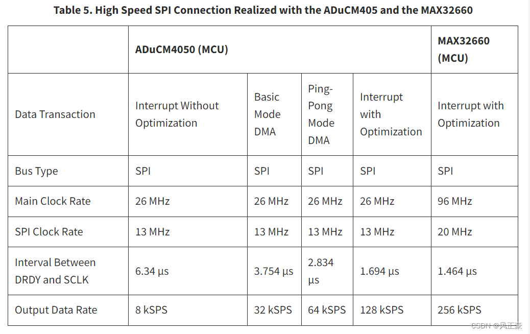
Assume the user is now reading the 200 24-bit ADC output data. The SPI bit rate is set at 13 MHz. We connect the pin with the DRDY signal and SCLK to the oscilloscope. By observing the time interval between the DRDY signal and the start of the SPI data transaction (also DMA transaction), we can quantize the speed improvement in each method introduced in this article. For convenience, we refer to the time interval from the DRDY signal to the start of the SCLK signal as ∆t. For the 13 MHz SPI bitrate, the measured Δt are:
假设用户现在正在读取 200 个 24 位 ADC 输出数据。 SPI 比特率设置为 13 MHz。我们将带有 DRDY 信号和 SCLK 的引脚连接到示波器。通过观察 DRDY 信号和 SPI 数据事务(也称为 DMA 事务)开始之间的时间间隔,我们可以量化本文介绍的每种方法的速度改进。为了方便起见,我们将从 DRDY 信号到 SCLK 信号开始的时间间隔称为 Δt。对于 13 MHz SPI 比特率,测得的 Δt 为:
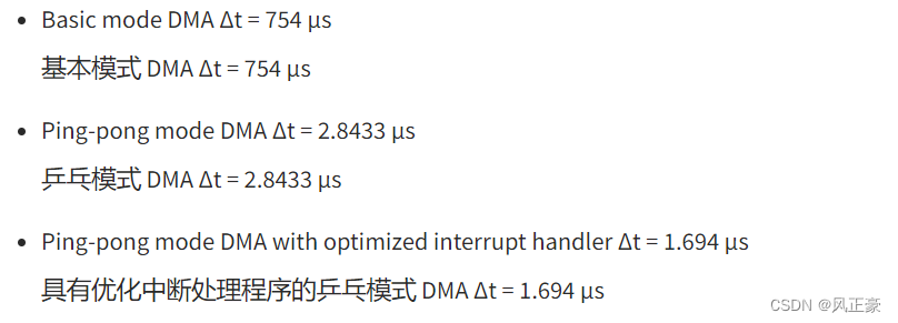
Methods (a) and (b) can support an ODR of 64 kHz while Method © can support an ODR of 128 kHz. This is because ∆t for Method © is the shortest, enabling SCLK to end earlier. If the SCLK signal—that is, data transaction—is done before the T/2 (T is the current ADC output data period), multiplication of the ODR will be available. Compared to the 8 kHz ODR speed performance of the ADI SPI driver, this can be seen as tremendous progress.
方法(a)和(b)可以支持64kHz的ODR,而方法©可以支持128kHz的ODR。这是因为方法©的Δt最短,使得SCLK能够更早结束。如果 SCLK 信号(即数据事务)在 T/2(T 是当前 ADC 输出数据周期)之前完成,则 ODR 的乘法将可用。与 ADI SPI 驱动器的 8 kHz ODR 速度性能相比,这可以看作是巨大的进步。
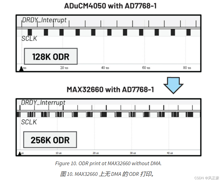
MAX32660 with the AD7768-1(MAX32660 与 AD7768-1)
What is the result when using the MAX32660, which is an MCU with 96 MHz of main clock rate? In this case, we used an interrupt data transaction with interrupt handler optimization. With this interrupt setup, a 256 kHz output data rate can be achieved without the DMA function. See Figure 10.
使用主时钟频率为96 MHz的MAX32660 MCU时,结果如何?在本例中,我们使用了带有中断处理程序优化的中断数据事务。通过此中断设置,无需 DMA 功能即可实现 256 kHz 输出数据速率。参见图 10。
Conclusion(结论)
With the selected ADC (AD7768-1) and MCU (ADuCM4050 or MAX32660), we can realize a high speed data transaction through SPI. To achieve the goal of speed optimization, we conduct the data transaction according to the ADI SPI driver but deduct the redundant commands. Also, the activation of the DMA controller frees the core and speeds up the continuous data transaction. With DMA ping-pong mode, DMA configuration time is saved with a proper schedule. On top of acceleration through DMA, the interrupt handler can also be optimized by direct specification of the interrupted pin. The best performance reaches a 128 kSPS ADC ODR at the 13 MHz SPI bit rate.
使用所选的ADC(AD7768-1)和MCU(ADuCM4050或MAX32660),我们可以通过SPI实现高速数据传输。为了达到速度优化的目标,我们根据ADI SPI驱动程序进行数据传输,但扣除了冗余命令。此外,DMA 控制器的激活可以释放内核并加速连续数据传输。使用 DMA 乒乓模式,可以通过适当的计划节省 DMA 配置时间。除了通过 DMA 加速之外,还可以通过直接指定中断引脚来优化中断处理程序。最佳性能在 13 MHz SPI 比特率下达到 128 kSPS ADC ODR。
Acknowledgments(致谢)
Throughout the writing of this dissertation, we have received a great deal of support and assistance.
在本论文的写作过程中,我们得到了很多支持和帮助。
We would like to thank Charles Lee, whose expertise was invaluable in hardware experience, software support, and even debugging tips.
我们要感谢 Charles Lee,他的专业知识在硬件经验、软件支持甚至调试技巧方面都是非常宝贵的。
We would also like to thank our mentor, William Chen, for his guidance in technical support.
我们还要感谢我们的导师 William Chen 在技术支持方面的指导。
Finally, we want to thank Frank Chang, who shared with us much of the technical experience from his career.
最后,我们要感谢 Frank Chang,他与我们分享了他职业生涯中的许多技术经验。
Note: All images and charts are courtesy of Analog Devices.
注:所有图像和图表均由 Analog Devices 提供。