Background
In order to meet the demand for multi-screen display from a single machine, the current system commonly uses the superframe/split mode to implement split screens. The general principle is as follows: the SOC side outputs a larger image (superframe), then the image is split into two screens (left and right) on the 941 side, and separately sent through port0 (DOUT0) and port1 (DOUT1) by FPD-Link III to the deserializer (948 Des) to achieve the purpose of split screen.

In the automotive industry, the temperature range requirement for device components is -40° to 120°. Components that can work normally within this temperature range can be considered as meeting automotive-grade requirements. Similarly, as an automotive-grade chip, 941 should also be able to meet this requirement.
Issue Symptom
During the testing process, it was found that before the temperature reached -40°, all boards would have no image output from port1, while the output from port0 was normal.
- After the problem occurred, power cycling the entire board did not resolve the issue.
- After the problem occurred, resetting and re-initializing the 941 alone did not resolve the issue.
- After the problem occurred, no output was observed regardless of writing a test pattern to either the 941 or 948.
- After the problem occurred, resetting the 941 alone and generating a test pattern using the internal clock of the 941 could successfully output the test pattern.
Issue Analysis
Possible Points of Suspicion
From the perspective of DSI signal transmission, the entire transmission chain is divided into the following parts:
- 8155->941
- 941 internal
- 941->948
For suspicion point 1, it's actually easy to rule out. Because the system outputs a superframe, which is a larger image for the 8155. If there is a problem with this part, then port0 should also be unable to display normally.
For suspicion point 2, it mainly involves hardware problems with the 941 and the configuration of internal registers in the 941, so it is the main focus of investigation.
For suspicion point 3, it can be directly ruled out after cross-validation (by swapping port0 and port1).
Analysis of Points of Suspicion
Suspected Point 2 can be roughly divided into:
Software issue
-Configuration of 941 registers, which is the main direction of investigation
Hardware issue
-Peripheral hardware issues of the 941.
a.MODE SEL issues, hardware engineers have tried various MODEs, but there is no effect, the problem remains.
b.Clock issues, tried to use an external crystal as the clock source, but it cannot match the requirements of the 941.
-Issues with the 941 chip itself.
Register Comparison Before and After the Problem
Before and after the problem occurred, we dumped the entire 941 main register, which can be referred to in the files port1_after.txt and port1_before.txt.
The main differences and analysis are as follows:
Part 1

0x0A:

This indicates that a CRC error occurred during the I2C read/write process.
0x0C:

Indicate that pixel clock is not detect on port1
Part 2

0x58:

Indicate that Line Video Error
0x5A:
indicate that DSI Frequency is NOT Stable AND No DSI Clock Detected for selected port.
0x5F:
Indicate that NO DSI Pixel Frequency.
Part 3
![]()
0x6D:
BCC error relate to I2C read/write
Part 4

0xC4:
0xC5:
0xC7:
There are No description for these registers on DS90UB941AS-Q1.pdf.
Analysis Conclusion
From above register analysis,We are very sure that the problem is related to the DSI clock.
Review register configuration on 941
Our register configuration as follow:
0x01,0x08,      //Disable DSI
0x1E,0x01,      //Select FPD-Link III Port 0
0x4F,0x0C,      //Set DSI_CONTINUOUS_CLOCK, 4 lanes, DSI Port 0
0x5B,0x07,      //Force Splitter mode
0x56,0x80,      //Enable Left/Right 3D processing to allow superframe splitting
0x1E,0x02,      //Select FPD-Link III Port 1
0x4F,0x0C,      //Set DSI_CONTINUOUS_CLOCK, 4 lanes, DSI Port 1
0x5B,0x07,      //Force Splitter mode
0x56,0x80,      //Enable Left/Right 3D processing to allow superframe splitting
0x32,0x80,      //Set the line size to 1920(LSB)
0x33,0x07,      //Set the line size to 1920 (MSB)
0x1E,0x01,      //Select FPD-Link III Port 1
0x36,0x00,      //Set crop start X position to 0 (LSB)
0x37,0x80,      //Set crop start X position to 0 (MSB) and enable cropping
0x38,0x7F,      //Set crop stop X position to 1919 (LSB)
0x39,0x07,      //Set crop stop X position to 1919 (MSB)
0x3A,0x00,      //Set crop start Y position to 0 (LSB)
0x3B,0x00,      //Set crop start Y position to 0 (MSB)
0x3C,0xCF,      //Set crop stop Y position to 719 (LSB)
0x3D,0x02,      //Set crop stop Y position to 719 (MSB)
0x1E,0x02,      //Select FPD-Link III Port 1
0x36,0x00,      //Set crop start X position to 0 (LSB)
0x37,0x80,      //Set crop start X position to 0 (MSB) and enable cropping
0x38,0x7F,      //Set crop stop X position to 1919 (LSB)
0x39,0x07,      //Set crop stop X position to 1919 (MSB)
0x3A,0x00,      //Set crop start Y position to 0 (LSB)
0x3B,0x00,      //Set crop start Y position to 0 (MSB)
0x3C,0xCF,      //Set crop stop Y position to 719 (LSB)
0x3D,0x02,      //Set crop stop Y position to 719 (MSB)
0x40,0x04,      //Select DSI Port 0 digital registers
0x41,0x05,      //Select DPHY_SKIP_TIMING register
0x30,0x01,  //Disable port1 remote interrupt due to we use same hw panel for touch interrupt
0x42,0x3C,      //Write TSKIP_CNT value for 300 MHz DSI clock frequency
0x01,0x00,      //enable DSI
The TI team didn't provide a split mode specific configuration, but we found a example code from Splitter Mode Operations With the 941.pdf.
After review these registers, We found an obvious problem:
From the description of 0x56:

We use DSI Reference Clock Mode now, so the BRIDGE_CTL:DSI_CONTINUOUS_CLK must be set(Red block). but the value for 0x4F is 0x0c:
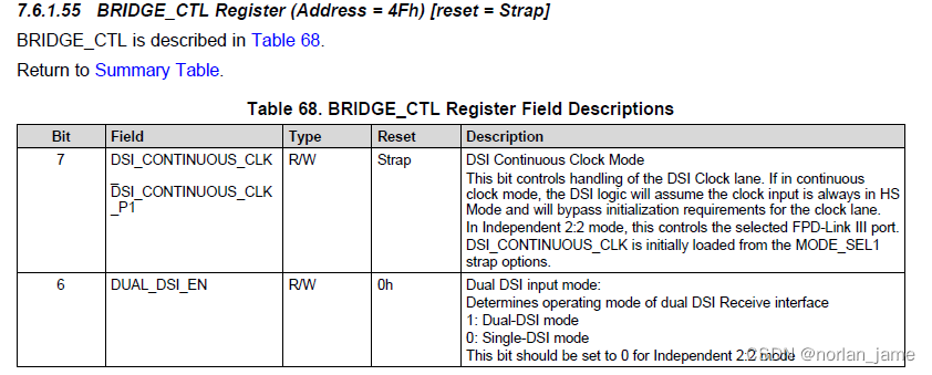
But the register description does not tell us how to enable DSI CONTINUOUS CLK(bit 7 = 1 means Continuous clock or bit 7 = 0 means Continuous clock?)
So we rise a case on e2e.ti.com for Ti and get their answer as follow:

refer to follow page to get detailhttps://e2e.ti.com/support/interface-group/interface/f/interface-forum/938509/ds90ub941as-q1-should-i-enable-dsi_continuous_clk-bit-when-using-split-mode
TI team have update their datasheet after this discussion.
Solution
Set 0x4F register to 0x8C to enable DSI CONTINUOUS CLOCK.
Please also make sure that your DSI clock from SOC is continuous. Read register HWIO_DSI_0_CPHY_MODE_CTRL_DLN0_CONTINUOUS_CLK_MODE_EN_BMSK on 8155 to confirm that or set flag sDeviceConfig.bEnableClkLaneHighPwrMode = TRUE in DSI driver to enable it. the register for 8155 is HWIO_DSI_0_LANE_CTRL_ADDR
if you want to configure it on Linux platform, please set "qcom,mdss-dsi-force-clock-lane-hs" in your dts file.
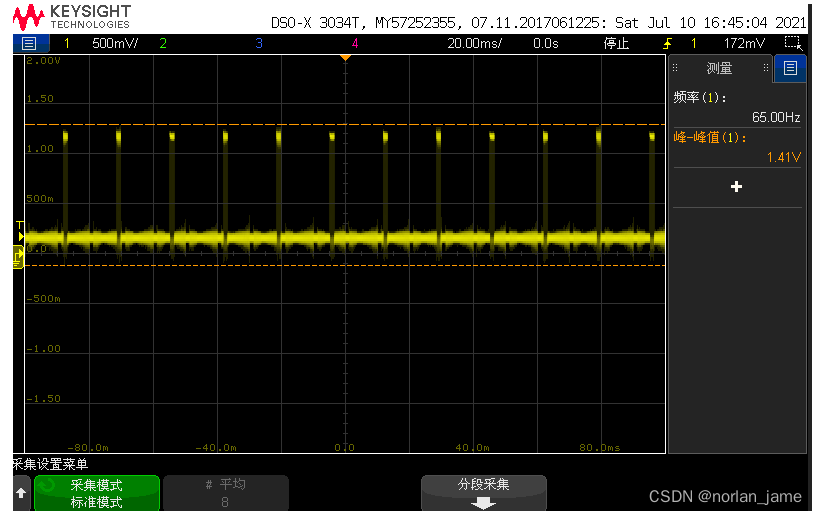
CONTINUOUS CLOCK sample (probing on DSI0_CLKP)

NON-CONTINUOUS CLOCK sample (probing on DSI0_CLKP)
Reference
Splitter Mode Operations With the 941.pdf
DS90UB941AS.pdf