VIVADO时序约束工具简要操作
项目简述
这里提醒,在看这篇文章之前一定要先把前一篇时序约束的文章看完,前面一篇才是重点,这篇就是一些简单的工具使用。
前面我们已经介绍了时序约束原理、参数的计算、Quartus II中时序约束方法。接下来,我们进行Xlinx的EDA工具VIVADO的时序约束方法。该约束方法我们将按照下图依次讲解,具体参数的计算我们在这篇博客中也将与前面的理论相联系。这篇博客中,我们分别进行原语、GUI的操作,使大家更容易明白其时序约束原理与时序参数。

基于原语的时序操作
首先这里需要注意的是,在进行时序约束之前一定要绑定引脚,否则进行的时序约束没有意义。
原语在Xlinx的工具中经常性的使用到。所谓的原语,同学们可以理解成为没有定制界面的IP,就给我们了一个顶层文件进而实现相应的功能。
时钟的约束
上面的时钟分为很多种情况,但是输入管脚是CLK、差分时钟、GT或恢复时钟是一类,另外的都属于生成时钟的种类。
输入时钟的约束
输入的时钟,使用以下原语进行约束:
create_clock -name <clock_name> -period <period> [get_ports <clock port>]
上面的 period 是时钟周期,clock port是输入时钟的管脚,clock_name是自己给这个时钟重新起的名字。
生成时钟的约束
生成时钟包括上面PLL等衍生时钟、自己分频的时钟。注意这里VIVADO对PLL的衍生时钟已经默认自己加了约束,当然我们也可以重新添加约束,约束是我们后添加的为准。
生成时钟的约束语句如下:
分频时钟:
# Generate a clock with a divided frequency from the master clock
# Generated frequency = master_clock_frequency / div_factor

create_generated_clock -name <generated_clock_name> \
                       -source <master_clock source_pin_or_port> \
                       -divide_by <div_factor> \
                       <pin_or_port>
上面generated_clock_name是我们对生成的时钟取得名字;master_clock source_pin_or_port这个是原时钟信号,对应于PLL的输入时钟;div_factor是分频的倍数;pin_or_port是生成的时钟信号。
倍频时钟:
# Generate a clock with a multiplied frequency from its master clock
# Generated frequency = master_clock_frequency * mult_factor

create_generated_clock -name <generated_clock_name> \
                       -source <master_clock source_pin_or_port> \
                       -multiply_by <mult_factor> \
                       <pin_or_port>
上面generated_clock_name是我们对生成的时钟取得名字;master_clock source_pin_or_port这个是原时钟信号,对应于PLL的输入时钟;mult_factor是倍频的倍数;pin_or_port是生成的时钟信号。
分数频时钟:
# Generated a clock with a fractional frequency of the master clock frequency:
# Generated frequency = master_clock_frequency * (mult_factor/div_factor)

create_generated_clock -name <generated_clock_name> \
                       -source <master_clock_source_pin_or_port> \
                       -multiply_by <mult_factor> \
                       -divide_by <div_factor> \
                       <pin_or_port>
上面generated_clock_name是我们对生成的时钟取得名字;master_clock source_pin_or_port这个是原时钟信号,对应于PLL的输入时钟;mult_factor是分频的倍数;div_factor是分频倍数;div_factor,pin_or_port是生成的时钟信号。
Input Delay约束
input delay的作用及计算方法在第一篇博客中我们已经进行了详细的说明。
定义1:input delay:我们在EDA软件中设置的input delay的值是以FPGA为中心,数据到达FPGA与时钟沿到达FPGA时间的差值。
由上面的定义,我们便可以得到input delay值得定义:
其实对于大多数PCB板做了等长处理,所以一般
与
相等,而且
在上游器件得技术手册中是给出得,一般命名为
,那么对于PCB板做了等长处理得器件,可以得下式:
以下所有的不同情况下约束都遵循上面的情况。
其实最简单的方法就是拿着示波器来测量FPGA输入引脚中时钟与数据的时间差值。
系统同步的Input Delay约束
系统同步的Input Delay约束SDR接收数据原语约束如下:
# Rising Edge System Synchronous Inputs
#
# A Single Data Rate (SDR) System Synchronous interface is
# an interface where the external device and the FPGA use
# the same clock, and a new data is captured one clock cycle
# after being launched
#
# input      __________            __________
# clock   __|          |__________|          |__
#           |
#           |------> (tco_min+trce_dly_min)
#           |------------> (tco_max+trce_dly_max)
#         __________      ________________
# data    __________XXXXXX_____ Data _____XXXXXXX
#

set input_clock     <clock_name>;   # Name of input clock
set tco_max         0.000;          # Maximum clock to out delay (external device)
set tco_min         0.000;          # Minimum clock to out delay (external device)
set trce_dly_max    0.000;          # Maximum board trace delay
set trce_dly_min    0.000;          # Minimum board trace delay
set input_ports     <input_ports>;  # List of input ports

# Input Delay Constraint
set_input_delay -clock $input_clock -max [expr $tco_max + $trce_dly_max] [get_ports $input_ports];
set_input_delay -clock $input_clock -min [expr $tco_min + $trce_dly_min] [get_ports $input_ports];

# Report Timing Template
# report_timing -from [get_ports $input_ports] -max_paths 20 -nworst 1 -delay_type min_max -name sys_sync_rise_in  -file sys_sync_rise_in.txt;
这里我们进行解释,系统同步SDR输入延迟约束:

因为是input delay的定义,所以可以知道:
所以从上图种可以看出:
当PCB布线等长时,上面的trce_dly_min与trce_dly_max等于0,所以结果也就是
这里也印证了我们之前博客中推导的正确性。
系统同步的Input Delay约束DDR接收数据原语约束如下:
# DDR System Synchronous Inputs
#
# A Double Data Rate (DDR) System Synchronous interface is
# an interface where the external device and the FPGA use
# the same clock, and a new data is captured half a clock
# cycle after being launched
#
# input      _______________________________                                  ________
# clock    _|                               |________________________________|
#           |                               |
#           |-> (trco_min+trce_dly_min)     |-> (tfco_min+trce_dly_min)
#           |-----> (trco_max+trce_dly_max) |-----> (tfco_max+trce_dly_max)
#          ____    ____________________________    ____________________________    ___
# data     ____XXXX__________Rise_Data_________XXXX__________Fall_Data_________XXXX___
#

set input_clock     <clock_name>;   # Name of input clock
set trco_max        0.000;          # Maximum clock to output delay from rising edge (external device)
set trco_min        0.000;          # Minimum clock to output delay from rising edge (external device)
set tfco_max        0.000;          # Maximum clock to output delay from falling edge (external device)
set tfco_min        0.000;          # Minimum clock to output delay from falling edge (external device)
set trce_dly_max    0.000;          # Maximum board trace delay
set trce_dly_min    0.000;          # Minimum board trace delay
set input_ports     <input_ports>;  # List of input ports

# Input Delay Constraint
set_input_delay -clock $input_clock -max [expr $trco_max + $trce_dly_max] [get_ports $input_ports];
set_input_delay -clock $input_clock -min [expr $trco_min + $trce_dly_min] [get_ports $input_ports];
set_input_delay -clock $input_clock -max [expr $tfco_max + $trce_dly_max] [get_ports $input_ports] -clock_fall -add_delay;
set_input_delay -clock $input_clock -min [expr $tfco_min + $trce_dly_min] [get_ports $input_ports] -clock_fall -add_delay;

# Report Timing Template
# report_timing -rise_from [get_ports $input_ports] -max_paths 20 -nworst 2 -delay_type min_max -name sys_sync_ddr_in_rise -file sys_sync_ddr_in_rise.txt;
# report_timing -fall_from [get_ports $input_ports] -max_paths 20 -nworst 2 -delay_type min_max -name sys_sync_ddr_in_fall -file sys_sync_ddr_in_fall.txt;
经过上面SDR的推导以及描述,相信大家很容易明白DDR数据在系统同步情况下的时序约束。
这里还没有介绍中心对齐的情况,因为包括上面的总共三种情况系统同步与源同步的约束语句完全相同这个直接参考源同步即可。
源同步的Input Delay约束
源同步SDR边缘对齐的Input Delay约束
# Edge-Aligned Rising Edge Source Synchronous Inputs
# (Using an MMCM/PLL)
#
# For an edge-aligned Source Synchronous interface, the clock
# transition occurs at the same time as the data transitions.
# In this template, the clock is aligned with the end of the
# data. The constraints below rely on the default timing
# analysis (setup = 1 cycle, hold = 0 cycle).
#
# input    __________                  ________________
# clock              |________________|                |__________
#                                     |
#                             skew_bre|skew_are
#                             <------>|<------>
#            _________________        |        _________________
# data     XX____Rise_Data____XXXXXXXXXXXXXXXXX_________________XX
#

set input_clock         <clock_name>;      # Name of input clock
set skew_bre            0.000;             # Data invalid before the rising clock edge
set skew_are            0.000;             # Data invalid after the rising clock edge
set input_ports         <input_ports>;     # List of input ports

# Input Delay Constraint
set_input_delay -clock $input_clock -max $skew_are  [get_ports $input_ports];
set_input_delay -clock $input_clock -min -$skew_bre [get_ports $input_ports];

# Report Timing Template
# report_timing -from [get_ports $input_ports] -max_paths 20 -nworst 1 -delay_type min_max -name src_sync_edge_rise_in  -file src_sync_edge_rise_in.txt;
查找上游器件的输出时序找到skew_bre与skew_are的值即可,或者经过滤波器测量。下面的还是原始定义:数据到达FPGA与时钟沿到达FPGA时间的差值。
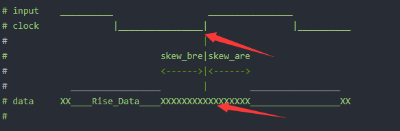
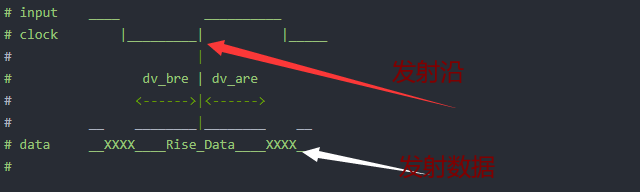
源同步SDR中心对齐的Input Delay约束:
# Center-Aligned Rising Edge Source Synchronous Inputs
#
# For a center-aligned Source Synchronous interface, the clock
# transition is aligned with the center of the data valid window.
# The same clock edge is used for launching and capturing the
# data. The constraints below rely on the default timing
# analysis (setup = 1 cycle, hold = 0 cycle).
#
# input    ____           __________
# clock        |_________|          |_____
#                        |
#                 dv_bre | dv_are
#                <------>|<------>
#          __    ________|________    __
# data     __XXXX____Rise_Data____XXXX__
#

set input_clock         <clock_name>;      # Name of input clock
set input_clock_period  <period_value>;    # Period of input clock
set dv_bre              0.000;             # Data valid before the rising clock edge
set dv_are              0.000;             # Data valid after the rising clock edge
set input_ports         <input_ports>;     # List of input ports

# Input Delay Constraint
set_input_delay -clock $input_clock -max [expr $input_clock_period - $dv_bre] [get_ports $input_ports];
set_input_delay -clock $input_clock -min $dv_are                              [get_ports $input_ports];

# Report Timing Template
# report_timing -from [get_ports $input_ports] -max_paths 20 -nworst 1 -delay_type min_max -name src_sync_cntr_rise_in  -file src_sync_cntr_rise_in.txt;
相信很多同学对这个不太了解。因为时中心对齐,上升沿是发射沿,那么发射数据是下一次数据突变的时刻。如下图:
那么min与max的关系如下:
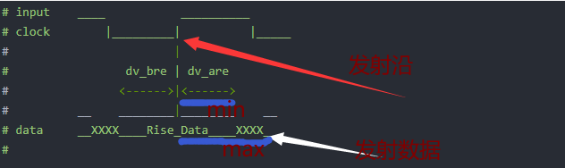
所以:
经过上面图文并茂的讲解,如果同学们还是不太了解,就查找一些其他的资料再和这个对比,相信同学们肯定可以弄懂这个,关键就是原始定义。
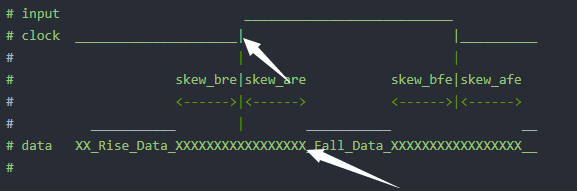
源同步DDR中心对齐的Input Delay约束:
# Edge-Aligned Double Data Rate Source Synchronous Inputs
# (Using an MMCM/PLL)
#
# For an edge-aligned Source Synchronous interface, the clock
# transition occurs at the same time as the data transitions.
# In this template, the clock is aligned with the end of the
# data. The constraints below rely on the default timing
# analysis (setup = 1/2 cycle, hold = 0 cycle).
#
# input                        ___________________________
# clock  _____________________|                           |__________
#                             |                           |
#                     skew_bre|skew_are           skew_bfe|skew_afe
#                     <------>|<------>           <------>|<------>
#          ___________        |        ___________                 __
# data   XX_Rise_Data_XXXXXXXXXXXXXXXXX_Fall_Data_XXXXXXXXXXXXXXXXX__
#

set input_clock         <clock_name>;      # Name of input clock
set skew_bre            0.000;             # Data invalid before the rising clock edge
set skew_are            0.000;             # Data invalid after the rising clock edge
set skew_bfe            0.000;             # Data invalid before the falling clock edge
set skew_afe            0.000;             # Data invalid after the falling clock edge
set input_ports         <input_ports>;     # List of input ports

# Input Delay Constraint
set_input_delay -clock $input_clock -max $skew_are  [get_ports $input_ports];
set_input_delay -clock $input_clock -min -$skew_bre [get_ports $input_ports];
set_input_delay -clock $input_clock -max $skew_afe  [get_ports $input_ports] -clock_fall -add_delay;
set_input_delay -clock $input_clock -min -$skew_bfe [get_ports $input_ports] -clock_fall -add_delay;

# Report Timing Template
# report_timing -rise_from [get_ports $input_ports] -max_paths 20 -nworst 1 -delay_type min_max -name src_sync_edge_ddr_in_rise -file src_sync_edge_ddr_in_rise.txt;
# report_timing -fall_from [get_ports $input_ports] -max_paths 20 -nworst 1 -delay_type min_max -name src_sync_edge_ddr_in_fall -file src_sync_edge_ddr_in_fall.txt;
从下面的DDR的图,相信大家联想input delay的定义可以得到input delay min与input delay max值得计算。
上面我们对input delay延迟分类做了详细论述,虽然不全,但是相信大家严抓定义肯定可以明白input delay得设置。
Output Delay约束
output delay得作用就是使下游器件满足时序要求,我们在讲解这个得时候需要严抓这个定义。 这里与input delay一样,系统同步与源同步其实本质上output delay min与output delay max得值是一样的,所以我们这里只拿源同步进行讲解。
源同步output delay约束
源同步SDR上升沿对齐的Onput Delay约束
#  Rising Edge Source Synchronous Outputs
#
#  Source synchronous output interfaces can be constrained either by the max data skew
#  relative to the generated clock or by the destination device setup/hold requirements.
#
#  Setup/Hold Case:
#  Setup and hold requirements for the destination device and board trace delays are known.
#
# forwarded         ____                      ___________________
# clock                 |____________________|                   |____________
#                                            |
#                                     tsu    |    thd
#                                <---------->|<--------->
#                                ____________|___________
# data @ destination    XXXXXXXXX________________________XXXXX
#
# Example of creating generated clock at clock output port
# create_generated_clock -name <gen_clock_name> -multiply_by 1 -source [get_pins <source_pin>] [get_ports <output_clock_port>]
# gen_clock_name is the name of forwarded clock here. It should be used below for defining "fwclk".

set fwclk        <clock-name>;     # forwarded clock name (generated using create_generated_clock at output clock port)
set tsu          0.000;            # destination device setup time requirement
set thd          0.000;            # destination device hold time requirement
set trce_dly_max 0.000;            # maximum board trace delay
set trce_dly_min 0.000;            # minimum board trace delay
set output_ports <output_ports>;   # list of output ports

# Output Delay Constraints
set_output_delay -clock $fwclk -max [expr $trce_dly_max + $tsu] [get_ports $output_ports];
set_output_delay -clock $fwclk -min [expr $trce_dly_min - $thd] [get_ports $output_ports];

# Report Timing Template
# report_timing -to [get_ports $output_ports] -max_paths 20 -nworst 1 -delay_type min_max -name src_sync_pos_out -file src_sync_pos_out.txt;
这是下游器件需要满足的建立时间与保持时间的要求:
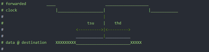
我们在第一篇时序分析的博客中推导output delay的约束为:
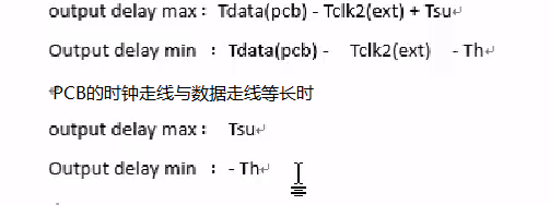
仔细观察两个结果其实是一样的。当PCB布线等长时,output delay的约束可以化简为:
这进而验证了我们前面讲解的正确性。
源同步SDR下降沿对齐的Onput Delay约束
#  Falling Edge Source Synchronous Outputs
#
#  Source synchronous output interfaces can be constrained either by the max data skew
#  relative to the generated clock or by the destination device setup/hold requirements.
#
#  Setup/Hold Case:
#  Setup and hold requirements for the destination device and board trace delays are known.
#
# forwarded                 _________________                    _______
# clock                ____|                 |__________________|
#                                            |
#                                     tsu    |    thd
#                                <---------->|<--------->
#                                ____________|___________
# data @ destination    XXXXXXXXX________________________XXXXX
#
# Example of creating generated clock at clock output port
# create_generated_clock -name <gen_clock_name> -multiply_by 1 -source [get_pins <source_pin>] [get_ports <output_clock_port>]
# gen_clock_name is the name of forwarded clock here. It should be used below for defining "fwclk".

set fwclk        <clock-name>;     # forwarded clock name (generated using create_generated_clock at output clock port)
set tsu          0.000;            # destination device setup time requirement
set thd          0.000;            # destination device hold time requirement
set trce_dly_max 0.000;            # maximum board trace delay
set trce_dly_min 0.000;            # minimum board trace delay
set output_ports <output_ports>;   # list of output ports

# Output Delay Constraints
set_output_delay -clock $fwclk -max [expr $trce_dly_max + $tsu] [get_ports $output_ports] -clock_fall;
set_output_delay -clock $fwclk -min [expr $trce_dly_min - $thd] [get_ports $output_ports] -clock_fall;

# Report Timing Template
# report_timing -to [get_ports $output_ports] -max_paths 20 -nworst 1 -delay_type min_max -name src_sync_neg_out -file src_sync_neg_out.txt;
下游器件需要满足的时序要求如下:
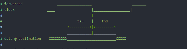
其实与上升沿相比只是约束的时候加了 -clock_fall来标志时下降沿触发。
源同步DDR下降沿对齐的Onput Delay约束:
#  Double Data Rate Source Synchronous Outputs
#
#  Source synchronous output interfaces can be constrained either by the max data skew
#  relative to the generated clock or by the destination device setup/hold requirements.
#
#  Setup/Hold Case:
#  Setup and hold requirements for the destination device and board trace delays are known.
#
# forwarded                        _________________________________
# clock                 __________|                                 |______________
#                                 |                                 |
#                           tsu_r |  thd_r                    tsu_f | thd_f
#                         <------>|<------->                <------>|<----->
#                         ________|_________                ________|_______
# data @ destination   XXX__________________XXXXXXXXXXXXXXXX________________XXXXX
#
# Example of creating generated clock at clock output port
# create_generated_clock -name <gen_clock_name> -multiply_by 1 -source [get_pins <source_pin>] [get_ports <output_clock_port>]
# gen_clock_name is the name of forwarded clock here. It should be used below for defining "fwclk".

set fwclk        <clock-name>;     # forwarded clock name (generated using create_generated_clock at output clock port)
set tsu_r        0.000;            # destination device setup time requirement for rising edge
set thd_r        0.000;            # destination device hold time requirement for rising edge
set tsu_f        0.000;            # destination device setup time requirement for falling edge
set thd_f        0.000;            # destination device hold time requirement for falling edge
set trce_dly_max 0.000;            # maximum board trace delay
set trce_dly_min 0.000;            # minimum board trace delay
set output_ports <output_ports>;   # list of output ports

# Output Delay Constraints
set_output_delay -clock $fwclk -max [expr $trce_dly_max + $tsu_r] [get_ports $output_ports];
set_output_delay -clock $fwclk -min [expr $trce_dly_min - $thd_r] [get_ports $output_ports];
set_output_delay -clock $fwclk -max [expr $trce_dly_max + $tsu_f] [get_ports $output_ports] -clock_fall -add_delay;
set_output_delay -clock $fwclk -min [expr $trce_dly_min - $thd_f] [get_ports $output_ports] -clock_fall -add_delay;

# Report Timing Template
# report_timing -rise_to [get_ports $output_ports] -max_paths 20 -nworst 2 -delay_type min_max -name src_sync_ddr_out_rise -file src_sync_ddr_out_rise.txt;
# report_timing -fall_to [get_ports $output_ports] -max_paths 20 -nworst 2 -delay_type min_max -name src_sync_ddr_out_fall -file src_sync_ddr_out_fall.txt;
这是下游器件要满足的时序信息:
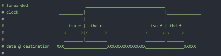
从这个图形来看,其实就是我们上面两个SDR的结合。
时序例外
为什么要用时序例外,什么条件下用时序例外,上一篇博客我们已经进行了讲解,这篇博客我们主要集中在原语操作中。
多周期路径的设置
建立时间:
set_multicycle_path <num cycles> -from <startpoints> -to <endpoints>
保持时间:
set_multicycle_path -hold <num cycles> -from <startpoints> -to <endpoints>
False路径的设置
set_false_path -from <startpoints> -to <endpoints>
VIVADO时序约束的GUI操作
首先要打开VIVADO的时序约束GUI界面,该GUI界面在综合和布局布线中都有选项,对于时序分析与约束我们一般在布局布线之后进行操作。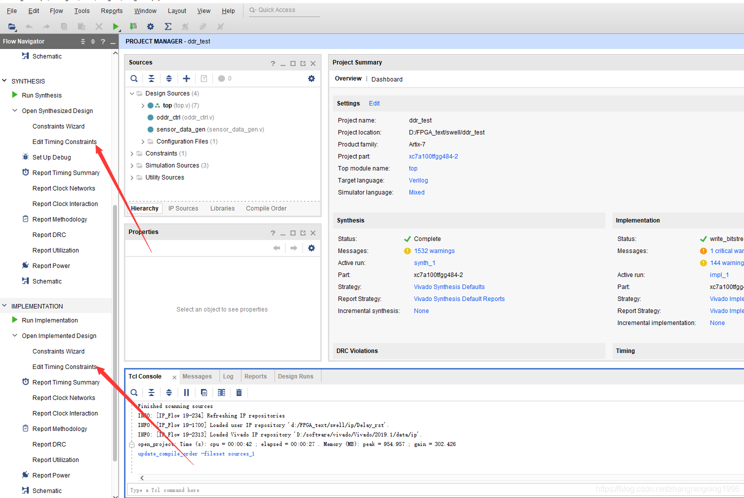
双击Edit Timing Constraints如图:
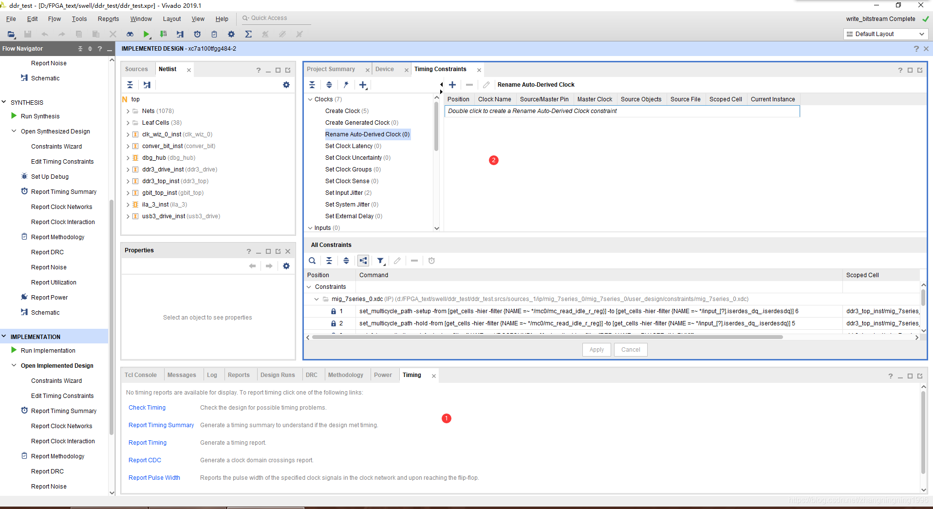
1、时序分析操作界面
2、时序约束界面

报到特定路径的时序。
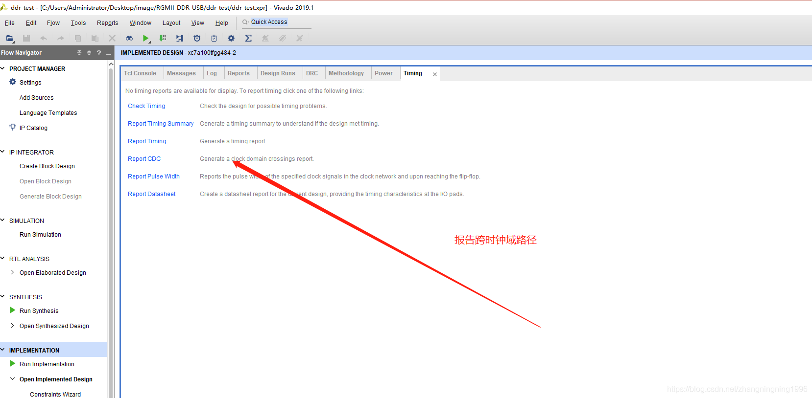
报告存在的跨时钟域约束。
1、设置输入时钟约束
2、设置生成时钟约束
3、设置输入延迟
4、设置输出延迟
5、设置False路径
6、设置多周期路径
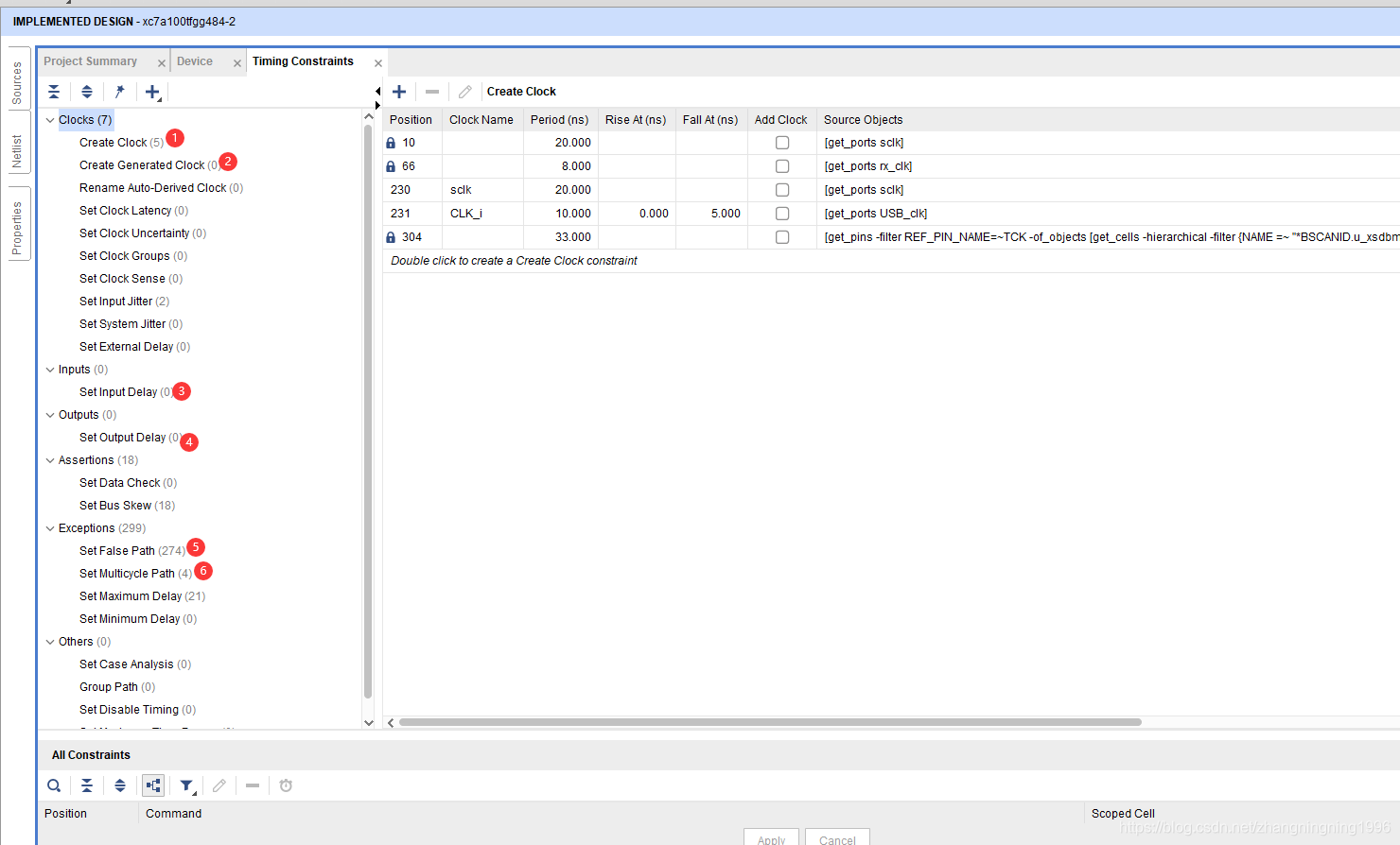
时钟的约束
时钟约束的位置如下:
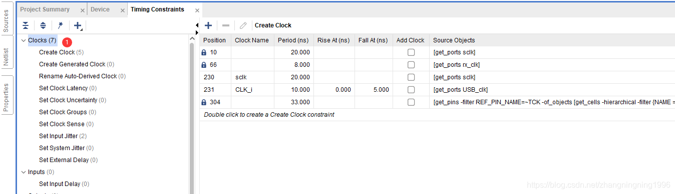
输入时钟的约束

1、时钟引脚的名字
2、找到时钟的信号
生成时钟的约束
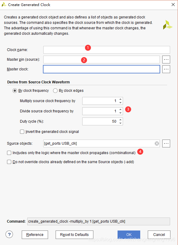
1、创建生成时钟的名字
2、指定生成时钟的源时钟
3、指定生成时钟与源时钟的分倍频关系
4、指定生成时钟信号
Input Delay约束
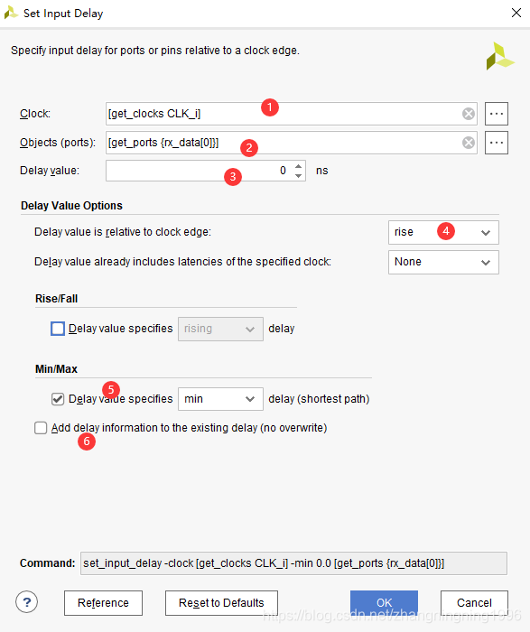
1、输入数据延迟时相对于哪一个时钟来说,这也就说明了输入延迟,首先应该约束数据的随路时钟
2、输入延迟的信号,一般时多选
3、输入延迟值
4、延迟值是针对上升沿还是下降沿来说的
5、该延迟设置的最大还是最小值
6、DDR的下降沿的时候勾选该选项,使得上升沿与下降沿的延迟同时存在
大家根据相应的类型勾选即可,也可以把生成的约束命令与原语相互比较。
output Delay约束
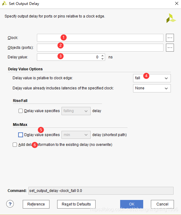
1、输出数据延迟时相对于哪一个时钟来说,这也就说明了输出延迟,首先应该约束数据的随路时钟
2、输出延迟的信号,一般时多选
3、输出延迟值
4、延迟值是针对上升沿还是下降沿来说的
5、该延迟设置的最大还是最小值
6、DDR的下降沿的时候勾选该选项,使得上升沿与下降沿的延迟同时存在
大家根据相应的类型勾选即可,也可以把生成的约束命令与原语相互比较。
时序例外
设置多周期路径
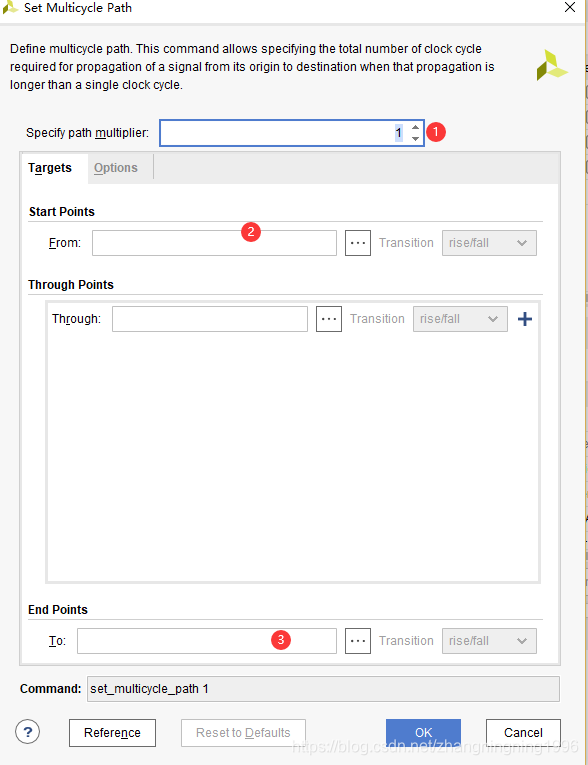
1、设置多周期的个数
2、设置源时钟
3、设置目的时钟
设置False路径
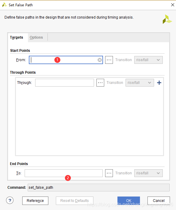
1、源端口(包括时钟或者信号)
2、目的段就(包括时钟或信号)
VIVADO时序操作策略
VIVADO、ISE、Quartus都有不同的优化策略,这些优化策略在一定程度上可以改善代码的时序性能,这也是时序约束中的重点。
总结
接触了FPGA已经两年时间,直到现在才敢说自己掌握了静态时序分析,学习过程可以说非常坎坷,因为当时的学习资料太少。创作不易,认为文章有帮助的同学们可以关注、点赞、转发支持。为行业贡献及其微小的一部分。或者对文章有什么看法或者需要更近一步交流的同学,可以加入下面的群: