Chapter 1 Industry Overview
1.1 Overview
Packaging is an important step in the semiconductor manufacturing process. In this step, semiconductor chips (or integrated circuits) are encased in a protective casing. The main function of this housing is to protect the chip from physical and chemical damage, such as protecting the chip from environmental factors such as moisture, dust, and temperature changes. The packaging process also involves connecting the chip to other electronic components, such as connecting the chip to a circuit board via leads or pads.
Advanced Packaging (Advanced Packaging) refers to emerging and high-tech packaging technologies designed to meet the needs of higher performance, smaller size, lower power consumption, and higher integration. These technologies include 3D Packaging, Chip Scale Packaging, 2.5D and 3D integration, etc. These technologies allow for tighter integration that can improve the performance and power efficiency of electronic devices while reducing size and weight. As a result, advanced packaging technologies find widespread use in many high-performance and miniaturized applications, such as mobile devices, high-performance computing, and the Internet of Things.
Figure: Simple comparison between advanced packaging and traditional packaging
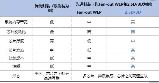
Source: Asset Information Network Qianji Investment Bank AVIC Securities
Advanced packaging has become a key technology to integrate more functions into various devices such as mobile phones and automobiles. It can achieve high device density in a small space, combining and packaging multiple devices such as electronic, mechanical or semiconductor devices into single electronic device. The global semiconductor advanced packaging market is expected to grow at a compound annual growth rate (CAGR) of 7.65% between 2021 and 2029 and is expected to exceed USD 61.69 billion by 2029, an increase from USD 34.62 billion in 2021. The key factors driving the growth of this market are the complexity of semiconductor integrated circuit (IC) design and the increasing number of functions and features being integrated into consumer electronic devices.
Integration of semiconductor components in automobiles will drive the growth of the global semiconductor advanced packaging market. The increasing demand for vehicle electrification and vehicle automation is driving the semiconductor market in this segment. For example, semiconductor ICs are used in multiple functions in automobiles, such as airbag control, GPS, anti-lock braking systems, display screens, infotainment systems, power windows, autonomous driving, and collision detection technology. In addition, semiconductor packaging technology is expected to increase the value of semiconductor products by increasing their operational functions, improving and maintaining performance, while reducing the overall cost of packaging. This has also created demand for high-performance chips for various consumer electronics products, thereby increasing the demand for 3D and 2.5D packaged chips used in smartphones and other mobile devices.
In China, about 1.425 million 5G base stations have been installed so far, supporting more than 500 million 5G users nationwide, making it the largest network in the world. The rapid development of 5G in this region is expected to drive the demand for 5G equipment, thereby increasing the demand for semiconductor packaging.
1.2 Development history
The historical development of packaging can be roughly divided into five stages:
(1) Through-Hole Mounting: This is the earliest stage of semiconductor packaging, mainly used in early integrated circuits and semiconductor equipment. At this stage, the pins of the packaged device are inserted through the holes in the circuit board and secured by soldering. The main advantage of this package type is its simple and stable structure, but its large size cannot adapt to the trend of miniaturization and high density.
(2) Surface-Mount Technology (SMT): As the size of electronic equipment shrinks and functions become more complex, surface-mount technology has begun to be widely used. This packaging method mounts the semiconductor device directly on the surface of the circuit board, eliminating the need to pass through the hole of the circuit board. This packaging method allows for smaller device sizes, higher densities, and higher production efficiency.
(3) Ball Grid Array (BGA): Ball Grid Array packaging technology emerged as the semiconductor industry continued to develop. This packaging method forms a ball-shaped pin array on the bottom of the device, which can provide more connection points and adapt to more complex integrated circuit designs. BGA packages provide better electrothermal performance and signal integrity, and are widely used in high-performance electronic devices.
(4) Multi-Chip Packaging (MCP): As the functions of electronic equipment continue to increase, multi-chip packaging technology has begun to be adopted. This packaging technology can integrate multiple semiconductor chips in one package, thereby achieving a higher degree of functional integration. This encapsulation method can reduce the connection length between devices and improve the performance and signal transmission speed of devices.
(5) Three-dimensional structure type (3D Packaging): This is the most advanced packaging technology at present. It uses a three-dimensional structure to stack multiple semiconductor chips together to form a three-dimensional integrated circuit. This packaging method can greatly improve the density and performance of integrated circuits, while reducing the delay of signal transmission, but its design and manufacturing process is relatively complicated and requires higher technical requirements.
Figure: Development history of integrated circuit packaging
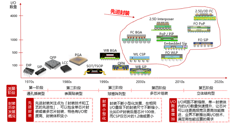
Source: Asset Information Network Qianji Investment Bank Yole
1.3 Classification
Advanced packaging is judged by the advanced nature of the internal packaging process, and can be divided into two categories based on the presence or absence of a substrate for internal connections. The division point of advanced packaging lies in the advanced nature of the process and packaging technology. Generally speaking, the package whose internal package is lead frame (WB) is not classified as advanced packaging, while the internal package uses flip-chip (FC), wafer-level (WL) ) and other advanced technology packaging can be called advanced packaging. Advanced packaging can be divided into two parts based on whether the internal connection has a carrier (substrate):
(1) Carrier (substrate type): The internal package needs to rely on the substrate, lead frame or interposer (Interposer), the main internal interconnection is flip-chip packaging (FC), which can be divided into single-chip or multi-chip packaging, multi-chip packaging There will be multiple chips side by side or stacked on the interposer (or substrate) to form a 2.5D/3D structure. The external packages under the substrate include BGA/LGA, CSP, etc. The packages are composed of internal and external packages. Currently, the industry The most representative and widely used combinations include FCBGA (Flip Chip BGA), Embedded SiP, 2.5D/3D Integration.
(2) No carrier (wafer level): no substrate, lead frame or interposer is required, so there is no distinction between internal and external packaging, represented by wafer level packaging, using redistribution layers (RDL) and bumps (Bumping), etc. are used as I/O winding means, and then directly connected to the PCB board in an upside-down manner, and the package thickness becomes thinner than that with a carrier. Wafer-level packaging is divided into fan-in (Fan-in) and fan-out (Fan-out), and fan-out can be extended to 3D FO packaging. Wafer-level packaging is the most advanced technology category in current packaging technology. .
Figure: Advanced Packaging Classification and Structure Diagram

Source: Asset Information Network Qianji Investment Bank Yole
Advanced packaging focuses on reducing size, system integration, increasing the number of I/Os, and improving heat dissipation performance. It can include single-chip and multi-chip. Flip-chip packaging and wafer-level packaging are widely used, and interconnection technology ( TSV, Bump, etc.) to improve the technical capabilities and promote the progress of packaging, internal and external packaging can be combined to form different high-performance packaging products.
Chapter 2 Business Model and Technology Development
2.1 Industry chain
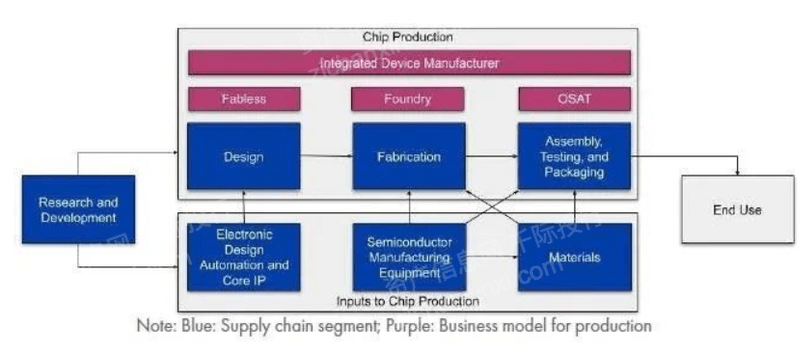
The industrial chain of the advanced packaging industry usually includes the following links:
- Design: In this phase, design engineers design semiconductor products based on product specifications and performance requirements. This may involve circuit design, physical design, and packaging design.
- Manufacturing: After the design is completed, it will enter the manufacturing stage. This typically includes wafer fabrication and wafer dicing. Wafer fabrication is mostly done by semiconductor equipment and material suppliers, while wafer dicing is done by semiconductor manufacturers such as TSMC or Intel.
- Packaging and testing: After the manufacturing process is complete, the chip needs to be packaged to protect its circuitry and provide electrical connections. After packaging, functional and performance testing is also required to ensure that the performance of the chip meets the design specifications.
- System Integration: Packaged chips will be integrated into electronic systems, such as mobile phones, computers, cars, etc. This step is usually done by original equipment manufacturers (OEMs) and manufacturing service providers (EMS).
- Sales and Service: Finally, the products that have completed the system integration will be sold to end users through various sales channels such as retailers or direct sales. Services may include product repairs and updates.
In this industrial chain, each link has specialized companies involved. For example, the design phase may be done by a design company, the manufacturing phase may be done by a semiconductor manufacturing company, the packaging and testing phase may be done by an packaging and testing service company (OSAT), system integration may be done by an OEM, and sales and service may be done by various retail companies. vendors and service providers.
Figure: Overview of Advanced Packaging Industry Chain
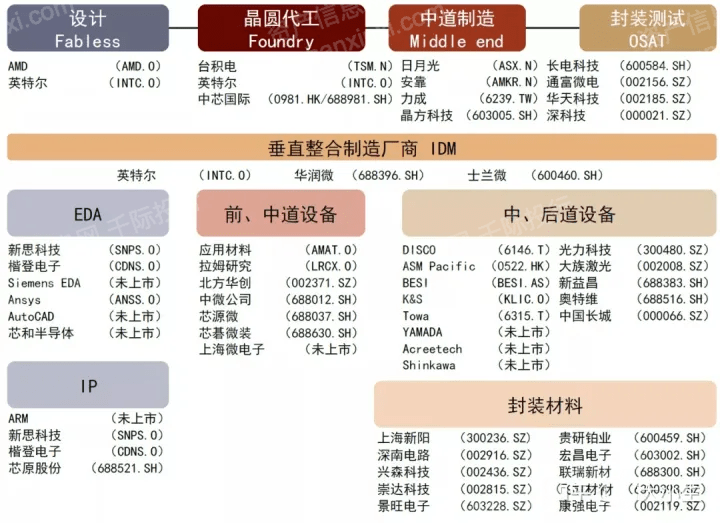
Source: Asset Information Network Qianji Investment Bank CICC
The upper reaches of the advanced packaging industry are packaging material suppliers represented by Kangqiang Electronics, Xingsen Technology, Dell Advanced Materials, and Sanhuan Group, and integrated circuit manufacturers represented by Silan Microelectronics and SMIC. As the main body of the integrated circuit packaging industry, the midstream mainly carries out the process of integrated circuit packaging and testing. The downstream is 3C electronics, industrial control and other terminal applications.
Figure advanced packaging upstream, midstream and downstream
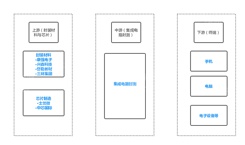
Source: Asset Information Network Qianji Investment Bank
upstream
With the development of packaging technology towards multi-pin, narrow pitch, and miniaturization, packaging substrates have gradually replaced traditional lead frames as mainstream packaging materials. Wire-bonded substrates account for about 40% to 50% of the total packaging cost, while flip-chip substrates account for as much as 70% to 80%. Compared with other packaging materials, packaging substrates are more difficult, but have high profits, numerous application fields, and broad market space.
Figure semiconductor packaging material standard

Source: Asset Information Network, Qianji Investment Bank, Founder Securities
The advanced packaging material market is relatively fragmented. Chinese companies have a certain influence in the bonding wire, epoxy molding compound, and lead frame markets, and the localization rate is relatively high, but there is a gap with international leading companies in terms of packaging substrates and chip bonding materials. Still larger.
With the emergence of new high-density packaging forms, many functions of electronic packaging, such as electrical connection and physical protection, are gradually being partially or fully undertaken by the packaging substrate. In recent years, high-density multilayer substrates account for an increasing proportion of electronic substrates, and they are more and more widely used in advanced packaging. As a special printed circuit board, the packaging substrate is a basic component that connects a higher-precision chip or device with a lower-precision printed circuit board. Compared with the parameters of line width/line spacing of 50μm/50μm on the PCB board, the packaging substrate can achieve parameters of line width/line spacing <25μm/25μm. The cost of the overall refinement of the PCB board is much higher than the cost of interconnecting the PCB and the chip through the packaging substrate.
Figure Semiconductor Packaging Substrate Market Trends
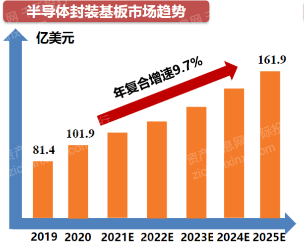
Source: Asset Information Network, Qianji Investment Bank, Founder Securities
middle reaches
Advanced packaging can usually be divided into metal packaging, ceramic packaging, and plastic packaging according to the shell material; according to the packaging link structure, it can be divided into internal packaging, external packaging and wafer-level packaging. board), including wire bonding (WB), tape automatic welding (TAB), flip-chip packaging (FC), and the external package is between the lead frame (or carrier board) and the printed circuit board (PCB) The connection method is the appearance of the package that we can see with the naked eye, such as QFP, QFN, BGA, LGA, etc. Some wafer-level packages are directly connected to the PCB board because they do not require a lead frame or a wire carrier, so they are out of the traditional internal and of the external package.
Figure: Basic situation of advanced packaging materials

Source: Asset Information Network Qianji Investment Bank Oriental Fortune Securities
downstream
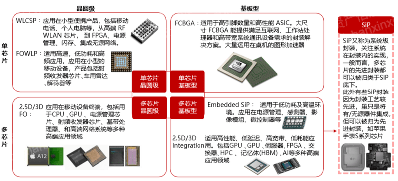
The downstream applications of advanced packaging mainly require mobile devices, multi-pin, and high-performance products. Wafer-level packaging is mostly used in small mobile devices, substrate type is mostly used in products with many pins and no volume limit, and multi-chip can be classified as SiP packaging.
Advanced packaging can be composed of single chip, multi-chip, wafer level, and substrate level. The difference between wafer level and substrate level comes from the difference in manufacturing process. Wafer level packaging is used in the chip manufacturing process and requires deposition , photolithography, deglue, etching and other processes. Compared with substrate-level packaging, wafer-level packaging can have a smaller packaging volume, so it is mostly used in small mobile devices, while substrate-level packaging is mostly used in high pins without volume restrictions. The product.
Figure: Advanced Packaging Applications
Source: Asset Information Network Qianji Investment Bank CITIC Securities
Generally speaking, multi-chip packages form a subsystem inside the package, so multi-chips can be classified as SiP (System in Package, system-level packaging). SiP packages focus on the system implementation in the package, regardless of advanced Or not, as long as it can be self-contained, it can be called SiP, and SiP in the field of advanced packaging includes 2.5D/3D FO, Embedded, 2.5D/3D Integration and more advanced heterogeneous heterogeneous packaging (such as Apple Watch S series chips), etc.
2.2 Business model
Advanced packaging currently includes two business models: one is internal ATP services performed by IDMs and foundries after manufacturing; the other is OSAT companies for third-party customers. OSAT customers can include IDMs, fabless companies and foundries.
Figure: Semiconductor Ecosystem
Source: Asset Information Network Qianji Investment Bank CSET
Back in the 1960s, semiconductor manufacturers took advantage of labor costs and set up factories in Asia. Today, outside the US and Europe, leading companies involved in semiconductor manufacturing are headquartered in Singapore, Korea, Japan and China. Leading IDMs and foundries in Europe, the US, South Korea and China are also investing heavily in advanced packaging. However, China-based companies dominate the OSAT segment.
Materials and equipment are used by OSATs, IDMs, and foundries to assemble and package finished wafers. Companies headquartered in the United States, China, South Korea, and Japan account for the majority of the packaging market share when measured by sales. However, Asia is the clear leader when looking at the location of physical facilities. Recent statistics show that China leads in the total number of packaging equipment (220, including Taiwan 106), followed by the rest of Asia-Pacific (65), North America (35), Japan (27) and Europe (19). The US- and Europe-based Semiconductor Industry Association estimates that at least 81% of the world's ATP production capacity is located in Asia.
2.3 Technology Development
Advanced packaging technologies include flip chip (Flip Chip), wafer level packaging (WLP), 2.5D packaging (Interposer), 3D packaging (TSV), Chip let, etc.
Figure: Summary of Advanced Packaging Technologies
Source: Asset Information Network Qianji Investment Bank CEIA Electronic Manufacturing
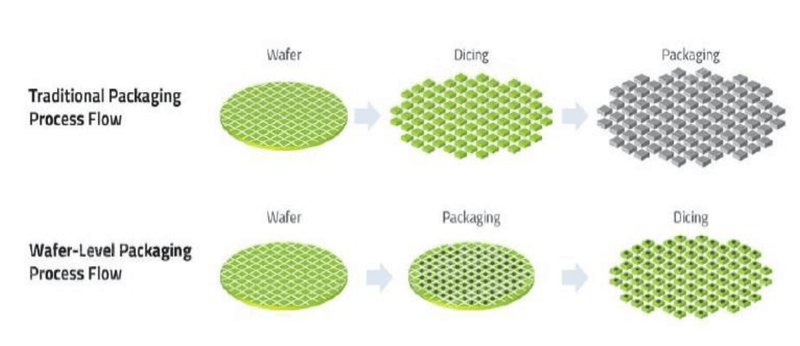
WLP (Wafer Level Package): Wafer Level Package
WLP is to directly carry out most or all of the packaging and testing procedures on the wafer, and then cut it into individual chips. With this packaging technology, there is no need for lead frames, substrates and other media, the packaging size of the chip is reduced, and the batch processing also greatly reduces the production cost. WLP can be divided into fan-in wafer level packaging (Fan-In WLP) and fan-out wafer level packaging
(Fan-Out WLP) two categories:
(1) Fan-in type: package directly on the wafer, cut after the package is completed, and the wiring is completed within the chip size, and the package size is the same as the chip size;
(2) Fan-out type: Based on the wafer reconfiguration technology, the diced chips are rearranged on the artificial carrier board. The distance between the chips depends on the requirements, and then wafer-level packaging is performed, and finally dicing is performed. On-chip and off-chip, the resulting package area is generally larger than the chip area, but the number of available I/Os increases.
Figure: WLP wafer level packaging
Source: Asset Information Network Qianji Investment Bank Jinghua Technology
Figure: Fan-in and fan-out packaging

Source: Asset Information Network Qianji Investment Bank Siliconware (SPIL)
Flip Chip: flip chip
Flip-chip process: refers to the direct deposition on the I/O pad of the chip, or the deposition of bumps (Bump) after RDL wiring, and then the chip is turned over and heated to combine the molten solder with the substrate or frame. Chip electrical face down.
Bump process: Necessary for the flip chip process. Planting tin balls or copper blocks on the surface of the wafer is one of the core technologies of advanced packaging.
2.5D packaging and 3D packaging
(1) 2.5D packaging: Dies are placed side by side on top of an interposer with through-silicon vias (TSVs). Its base, the interposer, provides the interconnection between the chips.
(2) 3D packaging: also known as stacked chip packaging technology, 3D packaging can use bumps or through silicon via technology (Through Silicon Via, TSV), TSV is a method of using vertical silicon vias to complete the interconnection between chips, because The connection distance is shorter and the strength is higher, enabling smaller and thinner packaging with better performance, higher density, significantly reduced size and weight, and it can also be used for interconnection between dissimilar chips.
SiP: System in Packag, system-in-package
SIP integrates a variety of functional chips, including processors, memory, FPGA and other functional chips, into one package to achieve a basically complete function. Corresponding to System on Chip (SoC), the difference is that System-in-Package is a packaging method in which different chips are used side by side or stacked, while SoC is a highly integrated chip product.
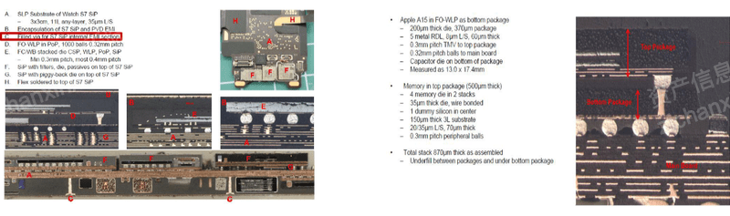
Figure: Advanced packaging technology used in Apple S7 watch and A15 chip
Source: Asset Information Network Qianji Investment Bank Prismark
Chiplet
Chiplet technology is a packaging form that realizes heterogeneous integration through bus and advanced packaging technology.
Figure: Chiplet

Source: Asset Information Network Qianji Investment Bank CEIA Electronic Manufacturing
Through statistics on the number of patents of various patent applicants in the domestic advanced packaging industry, the top companies are: Changdian Technology, Shengyi Technology, Tongfu Microelectronics, Nationstar Optoelectronics, Cambrian, Shenzhen Technology, Zhengye Technology wait.
Figure TOP 10 patents of listed companies in the advanced packaging industry

Source: Qianji Investment Bank iFinD
2.4 Policy Supervision
Administrative Supervision Department
(1) Ministry of Industry and Information Technology: mainly responsible for researching and formulating informatization development strategies, principles and policies, and overall planning; promoting strategic adjustment, optimization and upgrading of industrial structure; drafting industry laws and regulations, issuing administrative regulations, and organizing the formulation of industry technical policies and technical systems and technical standards, and macro-control the development direction of the industry.
(2) Ministry of Science and Technology: Mainly responsible for formulating national innovation-driven development strategies, scientific and technological development, introduction of foreign intellectual plans and policies, and organizing their implementation; leading the establishment of a unified national science and technology management platform and scientific research project funding coordination, evaluation, and regulatory agencies; drafting national Basic research plans, policies and standards and organize their implementation; formulate plans for major national science and technology projects and supervise their implementation; lead the construction of the national technology transfer system, formulate relevant policies and measures for the transfer and transformation of scientific and technological achievements and promote the combination of industry, academia and research, and supervise their implementation, etc.
self-regulatory association
(1) China Semiconductor Industry Association: It is a self-regulatory organization and coordination organization of the industry. It has professional institutions such as the Integrated Circuit Branch, the Semiconductor Discrete Device Branch, the Semiconductor Packaging Branch, and the Integrated Circuit Design Branch. The association is mainly responsible for implementing relevant government policies, Laws and regulations, put forward consultation opinions and suggestions on the economic, technical and equipment policies of the industry development to the competent government business department; do a good job in information consultation; investigate, research, and predict the industry and market, gather the requirements of enterprises, and reflect the voice of industry development; extensively carry out Economic and technological exchange and academic exchange activities; carry out international exchanges and cooperation; formulate (revise) industry standards, national standards and recommended standards and other tasks.
(2) China Electronic Special Equipment Industry Association: mainly responsible for providing industry surveys, market trends, economic operation forecasts and other information to member units and government authorities; on behalf of member units, put forward industrial development suggestions and opinions to government departments; do a good job in policy orientation , information-oriented, market-oriented work; widely carry out economic and technological exchanges and academic exchange activities, develop contacts with foreign groups, promote industrial development, and promote industrial internationalization, etc.
(3) China Integrated Circuit Testing Instrument and Equipment Industry Technology Innovation Alliance: The Institute of Microelectronics of the Chinese Academy of Sciences is the supporting unit, and it is formed on a completely voluntary basis by my country's industry-university-research units engaged in integrated circuit testing technology. Adhering to the tenet of "openness, collaboration, sharing, and win-win", the alliance is driven by the needs of my country's integrated circuit testing industry, and relies on the talents, technologies and market resources of each member unit of the alliance to strengthen information exchange and sharing, carry out domestic and international cooperation, and integrate Test industrial resources, highlight the overall advantages of the alliance, enhance the role of alliance members, and jointly promote the technological innovation and industrialization of my country's integrated circuit testing instruments and equipment.
industry policy
Figure industry main policies

Source: Asset Information Network Qianji Investment Bank Guanyan Tianxia
Chapter 3 Industry Valuation, Pricing Mechanism and Global Leading Enterprises
3.1 Comprehensive financial analysis and valuation methods of the industry
For the financial analysis of the advanced packaging industry, we need to consider the following main financial indicators:
- Revenue Growth: Examining a company's annual or quarterly revenue growth rate can help us understand how the company is performing in the market and the demand for its products or services. For the advanced packaging industry, we can expect continued revenue growth as electronic devices demand more complex and smaller semiconductors.
- Profitability: Profitability is an important indicator of a company's operating efficiency. We can get an idea of a company's profitability by examining its profit margins, such as gross margin, operating margin, and net profit margin.
- Capital Expenditure: Since the advanced packaging industry requires a large investment in R&D and production equipment, capital expenditure is also an important financial indicator. We can understand the company's investment in technology research and development and production capacity improvement by looking at the company's capital expenditure data.
- R&D investment: In an industry with rapid technological development, R&D investment is very important. We can understand a company's investment in future growth by looking at its R&D spending.
- Market Share: Market share can help us understand a company's position in its industry. For the advanced packaging industry, market share can be measured by a company's sales or production volume.
- Financial health: We also need to consider the financial health of the company, such as its current ratio (a measure of a company's ability to pay off short-term debt) and debt ratio (a measure of a company's long-term solvency).
Chart: Index Performance
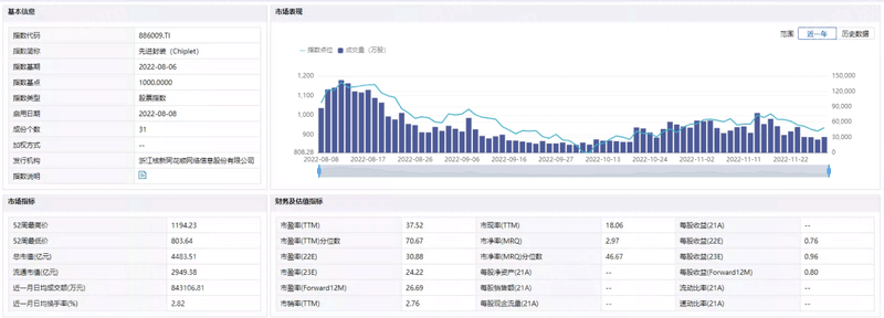

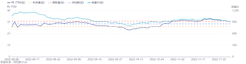
Source: Qianji Investment Bank iFinD
Valuation methods of the advanced packaging industry can choose price-earnings ratio valuation method, PEG valuation method, price-to-book ratio valuation method, price-to-cash ratio, P/S price-to-sales ratio valuation method, EV/Sales market-to-sales ratio valuation method, RNAV Revaluation net asset valuation method, EV/EBITDA valuation method, DDM valuation method, DCF discounted cash flow valuation method, NAV net asset value valuation method, etc.
Figure: JCET's main business
Figure: Main business of Tongfu Microelectronics

Source: Qianji Investment Bank iFinD
3.2 Industry Development and Driving Factors
Policy funding support
As the foundation and core of the information industry, the semiconductor industry is a strategic industry for national economic and social development, and the country has given great attention and strong support. In order to promote the development of my country's semiconductor industry, which is dominated by integrated circuits, and enhance the innovation capability and international competitiveness of the information industry, the state has issued a series of encouraging and supporting policies to establish an excellent policy environment for the advanced semiconductor packaging industry and promote the development of the advanced semiconductor packaging industry. Rapid development.
Transformation and upgrading of the integrated circuit industry
According to WSTS statistics, from 2017 to 2020, the global IC market size increased from US$343.19 billion to US$361.230 billion. In 2019, affected by Sino-US trade frictions, the total revenue of the global integrated circuit industry was US$333.35 billion, a decrease of 15.24% from 2018. With the easing of trade disputes, the gradual control of the global epidemic, and the continued vigorous development of emerging application fields such as 5G, Internet of Things, artificial intelligence, and wearable devices, the global IC industry market will return to growth in 2020, and it is expected to continue to grow in the future Situation In 2026, the global IC market size will increase to US$747.862 billion, of which IC design will reach US$277.457 billion; IC manufacturing will reach US$383.405 billion; IC packaging and testing will reach US$87 billion.

Source: Yidu Data of Qianji Investment Bank, Asset Information Network
The Rapid Rise of the Consumer Electronics Industry
The scale of production and sales of consumer electronics in my country ranks first in the world. my country is an important global manufacturing base for consumer electronics products. Most of the world's major electronics production and foundry companies have established manufacturing bases and R&D centers in my country.
Increasing number of industry-related engineers
3.3 Industry risk analysis and risk management
market risk
(1) Industry volatility risk
The integrated circuit industry is characterized by cyclical fluctuations, and the frequency of the semiconductor industry cycle is much higher than the economic cycle. During the upward or downward process of the economic cycle, a completely opposite semiconductor cycle may appear. Affected by the fluctuation cycle of the industry, it is uncertain whether the semiconductor industry can continue to recover in the future, which may have an adverse impact on the operating performance of the cash packaging and testing industry.
(2) Risk of industrial policy changes
The government's industrial policy on the integrated circuit industry provides a good policy environment for my country's advanced packaging and testing companies. If the national industrial policy changes unfavorably, it will have a certain impact on the industry. At the same time, the proportion of products sold abroad is relatively high. If the national industrial policy, import and export policy, or relevant policies, regulations or rules of the company’s product export countries or regions are adjusted, it may have an adverse impact on the company’s business. In addition, the company has factories in foreign countries, and changes in the country's industrial policies will also have an impact on the company's business operations.
Countermeasures: Companies in the industry should continue to pay attention to changes in market trends, macroeconomic conditions, relevant policies, and customer needs, and establish a benchmarking system to promptly adjust business development goals and investment directions to reduce the impact of relevant market risks.
business risk
(1) Risk of trade friction
Companies in the industry serve as manufacturing and testing companies for finished semiconductor chips. If the trade friction between the relevant countries and China continues to escalate, restrict imports and exports or increase tariffs, companies in the industry may face risks such as equipment and raw material shortages and customer loss, which will lead to limited production, reduced orders, and increased costs. operations are adversely affected.
Countermeasures: Companies in the industry should follow up the progress of trade disputes with relevant countries in a timely manner and disclose relevant information, and will actively take relevant countermeasures to reduce production and operation risks as much as possible.
(2) Equipment supply risk
The semiconductor chip manufacturing and testing industry has high requirements for equipment, and some important core equipment comes from overseas. In the future, some core equipment of companies in the industry may experience supply shortages and sharp price increases, or trade frictions, diplomatic conflicts, wars, etc. between the supplier’s country and region and China will affect the export license of the corresponding equipment, which may affect the The production, operation and sustainable development of the company are adversely affected.
Countermeasures: The company should actively take a series of measures such as promoting the diversification plan of the supply chain to minimize the adverse impact on production and operation caused by insufficient equipment supply.
(3) The risk of the epidemic affecting production and operation
Since the global outbreak of the epidemic in early 2020, most regions and industries have been affected to varying degrees. In the first half of this year, domestic epidemics have repeatedly occurred. During the epidemic, epidemic prevention and control measures such as isolation control and logistics restrictions may delay the company's personnel attendance, equipment procurement, installation and maintenance, sales and delivery, and market activities such as customer development will be restricted to a certain extent. The epidemic situation in the locations of customers and suppliers of companies in the industry will also affect the daily business activities of upstream and downstream companies in the industrial chain, thus adversely affecting the entire integrated circuit industry.
Countermeasures: Companies in the industry should continue to pay close attention to the development of the new crown epidemic, evaluate and actively respond to its impact on the company's financial status and operating results.
(4) Risk of intensified market competition
The demand for traditional consumer electronics has gradually slowed down from the first quarter of 2022, and the inventory level of IC end users, including mobile phone manufacturers, is significantly higher than that in 2021. There is a risk of a decline in semiconductor packaging and testing demand in the second half of the year; In the wide spread, superimposed international political events including the Russia-Ukraine war, together affect the supply chain, and then affect sales; when the market demand declines, the price competition brought about by the idle production capacity of some domestic packaging and testing, and then the sales of the industry and profit margins.
3.4 Competitive Analysis - Using SWOT Model
Advantage
Compared with traditional packaging, the new form is rapidly rewriting the characteristics of the packaging and testing industry, which is dominated by low-threshold, low-unit-price competition and a high degree of homogeneity. With the entry of IDMs (vertically integrated manufacturers) and fabs, the penetration of front-end and middle-of-the-road processes continues to raise the barriers to advanced packaging technologies. At the same time, advanced packaging highlights the integration and interconnection between chip devices. Designers need to consider the entire system-level design and optimization, including packaging, at the initial stage of chip development. Considering that advanced packaging brings more design points such as heat dissipation and mechanical mechanism, the service scope of EDA tools has been expanded. .
disadvantage
As chip designs become more heterogeneous and application-specific, the resulting changes become more problematic, making it difficult to determine the source of a problem or predict why and when it will go wrong. There are also differences in the bonding/debonding and interconnects used in advanced packaging. For example, harnesses with options for mass reflow soldering, thermocompression bonding, and laser-assisted bonding interconnects, or a combination of harnesses plus flip-chip and various passive components. For each process, there are many variations in temperature, stress residue and possible invisible microcracks.
opportunity
On the equipment side, although the packaging and testing industry is the most mature link in my country's semiconductor industry chain, the localization rate of back-end packaging and testing equipment and packaging materials is still low, and there is a lot of room for substitution. With the rapid development of Zhongdao manufacturing, domestic front-end equipment manufacturers have successfully entered the production lines of leading customers and have formed strong competitiveness. New opportunities are coming.
threaten
Global mainstream packaging and testing manufacturers are currently increasing investment in the field of advanced packaging, but domestic packaging is still dominated by traditional packaging. Changdian Technology and Tongfu Microelectronics have achieved industrialization capabilities for advanced packaging through independent research and development and mergers and acquisitions. A certain level, but China's advanced packaging accounts for about 25%, which is lower than the global level.
3.5 Important participating enterprises
Major Chinese companies include China Resources Microelectronics [688396.SH], Changdian Technology [600584.SH], Shengyi Technology [600183.SH], Shengmei Shanghai [688082.SH], Huatian Technology [002185.SZ], Fuweidian [002156.SZ], Cambrian [688256.SH], Zhenhua Scenery [688439.SH], VeriSilicon [688521.SH], Shenzhen Technology [000021.SZ], etc.
According to Yole Group, based on the company's sales revenue in high-performance chip manufacturing, including companies providing outsourced semiconductor assembly and testing (OSAT) services and DRAM manufacturers, the top 16 global advanced packaging companies in 2023 are: ASE Technology, Amkor Technology, JCET, TSMC, SPIL, Intel, Samsung Electro-Mechanics, Huatian Technology, Samsung, Unisem, KYEC, TFME, ChipMOS, Greatek Electronics, TongFu Microelectronics, UTAC.
Chapter 4 Future Outlook
The advanced packaging market is experiencing significant growth and is expected to continue growing in the coming years. The size of this market globally is expected to reach over USD 61 billion by 2029, at a CAGR of 7.65%. Key factors driving the growth of this market include the complexity of semiconductor integrated circuit (IC) design, and the need for miniaturized and high-performance semiconductors in automotive and consumer electronics.
Taiwan Semiconductor Manufacturing Company (TSMC), the world's largest contract chipmaker, is accelerating its investments in advanced packaging to meet the needs of the artificial intelligence field. According to reports, the company intends to accelerate investment and expansion in the field of advanced packaging as demand for advanced packaging solutions exceeds its current production capacity.
According to the Yole Group report, advanced packaging is increasing its share of the overall semiconductor market due to strong market trends. It has become the most attractive and dynamic business segment, attracting large companies at all levels of the supply chain. Yole Group predicts that the semiconductor packaging market will be worth more than $100 billion in the next five years, with industry giants such as TSMC, Intel and Samsung driving the development of advanced packaging.
The mobile and consumer markets are currently the major revenue generators for the advanced packaging market and are expected to grow at more than 8% annually over the next five years. Meanwhile, the automotive and broader transportation segments are the fastest growing segments of the advanced packaging market. The telecom and infrastructure segment also plays a key role in the advanced packaging industry, with growth similar to that of the mobile and consumer segments.
In the future, advanced packaging will drive unprecedented levels of investment. The demand for data processing continues to grow, and heterogeneous functions such as data storage, data processing, and sensing need to be integrated in the same package. As front-end manufacturing has boundaries in terms of performance and cost, packaging and advanced packaging provide the core elements that meet the needs of OEMs and module manufacturers, as well as integrated device manufacturers (IDMs).
Cover Photo by Vishnu Mohanan on Unsplash