overview
提示:这里可以添加技术概要
When building a signal chain solution for a precision data acquisition system, one of the greatest challenges in optimizing the signal is the challenge presented by managing the balance of noise between the signal chains. The gain size of the gain stage, whether the gain stage can directly drive the analog-to-digital conversion unit, the relationship between SNR and gain, and the role of digital filtering in the signal chain are all issues that design engineers often consider when building a data acquisition signal chain. These issues will be addressed in terms of noise tradeoffs.
This article mainly introduces the selection of buffer bandwidth size
overall architecture process
提示:这里可以添加技术整体架构
Taking the 20-bit ADC as an example, its valuation factor is 2 3, which will make the buffer frequency approximately nine times the Nyquist frequency. Using a first-order filter with a 40% duty cycle, the buffer rises from 9.3 times the Nyquist frequency to 14.7 times. The noise bandwidth of the buffer is 15 times that of the ADC. If the sampling duty cycle is reduced from 40% to 20% or 25%, the noise will be proportional to the bandwidth of the filter. Although the buffer noise spectral density is low, it has a relatively wide frequency band and is sampled folded down into the ADC bandwidth so that all noise folds from zero to the Nyquist frequency. If there is any external interference in the signal chain from the power supply or in the signal chain, these spurs are high frequency and will fold again, so it is extremely important to try to reduce the buffer bandwidth from a glitch amplitude perspective or a power supply interference suppression perspective, after all Buffer stages have wide bandwidth in the signal chain. In some low-end applications the ADC runs at a slower speed, such as a clock frequency of 5MSPS and not higher, at this speed there will be more time to stabilize the kickback, so the bandwidth of the buffer filter can be reduced
Explanation of technical terms
ADC:
An analog-to-digital converter, or A/D converter, or ADC for short, usually refers to an electronic component that converts an analog signal into a digital signal. A common analog-to-digital converter converts an input voltage signal into an output digital signal. Since the digital signal itself has no practical significance, it only represents a relative size. Therefore, any analog-to-digital converter needs a reference analog quantity as a conversion standard, and the more common reference standard is the largest convertible signal size. The output digital quantity represents the magnitude of the input signal relative to the reference signal
Signal sampling:
Sampling refers to the process of extracting individuals or samples from the population, that is, the process of conducting experiments or observations on the population. There are two types of random sampling and non-random sampling. The former refers to the sampling method that draws samples from the population according to the principle of randomization, without any subjectivity, including simple random sampling, systematic sampling, cluster sampling and stratified sampling. The latter is a method of drawing samples based on the researcher's point of view, experience or relevant knowledge, which is obviously subjective. See "Random Sampling", "Non-Random Sampling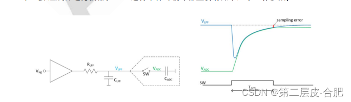
technical details
提示:这里可以添加技术细节
In some low-end applications where the ADC runs at a slower speed, such as a clock frequency of 5MSPS rather than higher, there will be more time for the kickback to stabilize at this speed, so the bandwidth of the buffer filter can be reduced. For some applications that need to increase the bandwidth of the buffer filter, there are generally two methods, one is to increase the resistance, and the other is to increase the capacitance, both of which have their own advantages and disadvantages:
1. Increase the capacitance,
Increasing the capacitance will lower the amplitude and the buffer will behave in a more linear fashion but is less likely to sample large signals. Of course, a smaller cap would result in lower filter noise on the other end, increasing AC load and power dissipation, and potentially causing driver instability.
2. Increase the resistance,
A five-fold increase in resistance results in a direct increase in distortion because all non-linear currents generated by the ADC are scaled by the resistance value. But the upside is that increasing the resistor reduces the load on the snubber, which not only prolongs driver life but also reduces AC power consumption.
summary
提示:这里可以添加总结
The noise spectral density amplitude and bandwidth of the modules at all levels in the signal chain are shown. The blue part is the gain stage, the orange part is the ADC, and the green part is the buffer stage. The noise spectral density of all analog front ends is referred to the ADC input, and for example purposes, the noise spectral density of the gain stage is limited to four times the signal frequency to achieve greater flatness in the passband. Compared to the ADC noise spectral density, the buffer stage noise spectral density is lower but the bandwidth is significantly wider, typically reaching 10 or 15 times the ADC noise frequency. The following sections will also explain why the buffer bandwidth is set wider.