content
Blocking assignment simulation
Comprehensive look at the RTL diagram
Non-blocking assignment simulation
Comprehensive look at the RTL diagram
blocking assignment
The assignment number of blocking assignment is represented by "=", and the corresponding circuit structure often has nothing to do with triggering Yan Ni, but is only related to the change of the input level. Its operation can be considered as a one-step operation, that is, calculating the statement on the right side of the assignment number and updating the statement on the left side of the assignment number. At this time, no interference from any other Verilog statement is allowed, and the next one is not allowed until the current assignment is completed. the execution of the assignment statement.
A serial block is also called begin end, and the blocking assignment statements are executed in the order in which they are listed in the sequential block.
non-blocking assignment
The assignment number of non-blocking assignment is represented by "<=", the corresponding circuit structure is often related to the trigger edge, and non-blocking assignment can be performed only at the moment of the trigger edge.
Its operation can be seen as a two-step process: at the end of the assignment, the statement to the left of the assignment number is updated.
Other Verilog statements are allowed to operate concurrently while the statement to the right of the assignment number of the non-blocking statement updates the statement to the left of the assignment number.
Non-blocking left slots can only be used for assignment to register type variables (reg), so they can only be used in "initial" and "always" blocks, and are not allowed for continuous assignment "assign".
Actual Engineering Simulation
Blocking assignment simulation
Write Verilog code
The first is blocking assignment simulation (blocking), using "=" for assignment, indicating blocking assignment.
module	blocking
(
	input	wire			clk,
	input	wire			rst_n,
	input	wire	[1:0]	in,
	output	reg		[1:0]	out

);

reg		[1:0]	in_reg;

always @(posedge clk or negedge rst_n) begin
	if (rst_n == 1'b0) begin
		in_reg = 2'b0;
		out    = 2'b0;
	end
	else begin
		in_reg = in;
		out    = in_reg;
	end
end
endmodule
Write test file code
`timescale 1ns / 1ns
module tb_blocking();
reg clk;
reg rst_n;
reg [1:0] in;
wire [1:0] out;
initial begin
clk = 1'b1;
rst_n <= 1'b0;
in <= 2'b0;
#20
rst_n <= 1'b1;
end
always #10 clk = ~clk;
always #10 in <= {$random} % 4;
blocking tb_blocking(
.clk(clk),
.rst_n(rst_n),
.in(in),
.out(out)
);
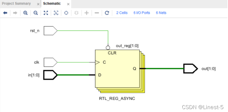
endmoduleComprehensive look at the RTL diagram
It can be seen that there is only one register, so the actual simulation diagram should show that the in_reg and out signals should change at the same time, and both signals are delayed by one beat of the in signal.
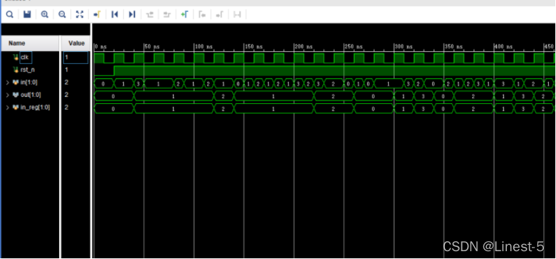
Do the actual simulation
as expected
Non-blocking assignment simulation
Write Verilog code
As follows: Just change the code of blocking assignment from "=" to "
module	blocking
(
	input	wire			clk,
	input	wire			rst_n,
	input	wire	[1:0]	in,
	output	reg		[1:0]	out

);

reg		[1:0]	in_reg;

always @(posedge clk or negedge rst_n) begin
	if (rst_n == 1'b0) begin
		in_reg <= 2'b0;
		out	   <= 2'b0;
	end
	else begin
		in_reg <= in;
		out    <= in_reg;
	end
end
endmodule
Write test file code
Same as the test file for blocking assignments
`timescale 1ns / 1ns

module tb_blocking();

	reg				clk;
	reg				rst_n;
	reg		[1:0]	in;

	wire	[1:0]	out;

	initial	begin
		clk = 1'b1;
		rst_n <= 1'b0;
		in <= 2'b0;
		#20
		rst_n <= 1'b1;
	end
	always #10 clk = ~clk;
	always #10 in <= {$random} % 4;


blocking tb_blocking(
	.clk(clk),
	.rst_n(rst_n),
	.in(in),
	.out(out)
	);
endmodule
Comprehensive look at the RTL diagram
It can be seen that there are two registers, one register is assigned from the in signal to the in_reg signal, and there is also a register that is assigned from the in_reg signal to the out signal, so the actual simulation diagram should show that the in_reg signal is delayed relative to the in signal. The time is one beat, and the out signal is delayed by one beat relative to the in_reg, that is, two beats relative to the in signal.

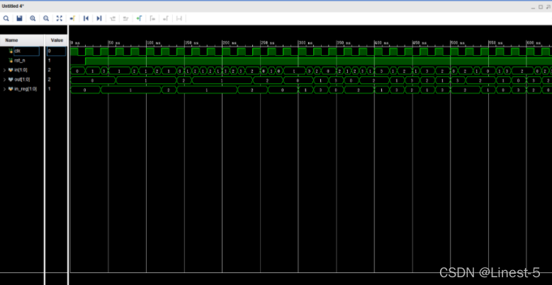
Actual simulation diagram
Consistent with what was assumed after observing the RTL plot.
Summarize
Blocking assignment and non-blocking assignment cannot be used indiscriminately in actual use, otherwise unpredictable consequences may occur. According to the official recommendations, when writing combinational logic circuits, use blocking assignment; when writing sequential logic, use non-blocking assignments. Blocking assignment.