Say "Fa" today: Who touched my JTAG port?
Welcome heroes to the new column of FPGA Technology Jianghu and say "Fa" today. Of course, here we are definitely not going to study and discuss knowledge of laws and regulations, so what are we discussing, here we are discussing some small things in product development and technology learning. For details, small methods, etc., everyone is welcome to learn and exchange together. If you have good inspiration and essays on the article, you are welcome to contribute. Please indicate your pen name and related articles. The submission recipient email: [email protected]. What I brought today was "Who touched my JTAG port?", not much to say, the goods are on sale.
In the process of FPGA research and development and learning, there is a key step to implement off the board. It is very important to make hardware "hard display". Generally speaking, it is more common to use the JTAG port. Therefore, I believe that some heroes must have encountered JTAG port failure or damage. Things that can't be used. I have encountered this kind of thing recently. The JTAG port of FPGA suddenly can’t download programs. And this kind of thing is not the first time. It has appeared in the project before, and the form of appearance is very similar. It's still used well, but it won't work the next day, which is really depressing. To this end, I also tried many solutions. I didn't even imagine that the JTAG port was broken at the beginning. So, I changed the usb-blaster, but there was no response at all. Is it true that the JTAG port is broken? So, I went to check the relevant information to figure out the essence of the problem. Here are some of my gains, and I will share them for your reference only and exchange and study together.

According to the information obtained and some of my practical experience, when using the JTAG download interface, please do not plug or unplug it with power at will, otherwise it will damage the JTAG port signal pins of the FPGA chip. So how to confirm that the JTAG port has been damaged. First of all, you have to eliminate several basic factors. One is whether to match the connection. There are many devices that correspond to many interfaces. Under actual conditions, it must be matched correctly, otherwise the above situation will also occur; the second is to eliminate the problem of the download line. If the download line is broken, you can use multiple download lines to try to eliminate this kind of problem. If you still cannot access the JTAG port of the FPGA, it is very likely that the JTAG port of your FPGA chip has been damaged. At this time, please use a multimeter to check whether TCK, TMS, TDO and Tdi are short-circuited to GND. If any signal is short-circuited to ground, it means that the JTAG signal pins have been damaged.
As for what the JTAG port is, let's also discuss it here. The full English name of JTAG is Joint Test Action Group, and the translated Chinese is Joint Test Action Group.
JTAG is an IEEE standard used to solve board-level problems and was born in the 1980s. Today JTAG is used for programming, debugging, and probing ports. Of course, the most primitive use is boundary testing.
1. Boundary test:
For example, if you have two chips, there are many wires connected between the two chips. How to ensure that the connection between these wires is OK? With JTAG, it can control all IC pins. This is called chip boundary testing.

2. JTAG pins:
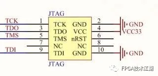
JTAG has developed to now have pins, usually four pins: TDI, TDO, TMS, TCK, of course, there is a reset pin TRST. The JTAG pins on the chip are actually dedicated.
-
TDI: Test data input, data is input to JTAG port through TDI;
-
TDO: Test data output, data is output from the JTAG port through TDO;
-
TMS: Test mode selection, used to set the JTAG port in a specific test mode;
-
TCK: Test clock input;
-
TRST: Test reset.

CPU and FPGA manufacturers allow JTAG to be used for port debugging; FPGA manufacturers allow the FPGA to be configured through JTAG and use JTAG signals to access the FPGA core.
3. How does JTAG work:
PC control JTAG: Use a JTAG cable to connect to the PC's print port or USB or network port. The easiest is to connect to the print port.
TMS: Inside each chip that contains JTAG, there will be a JTAG TAP controller. The TAP controller is a state machine with 16 states, and TMS is the control signal for this thing. When TMS connects the various chips together, the TAP state transitions of all chips are consistent. The following is a schematic diagram of the TAP controller:

Change the value of TMS, the state will jump. If you keep the high level for 5 cycles, it will jump back to test-logic-rest, which is usually used to synchronize the TAP controller; usually the two most important states are Shift-DR and Shift-IR, which are connected to TDI and Used by TDO.
IR: Command register. You can write a value to this register to tell JTAG to do something. Each TAP has only one IR register and its length is fixed.
DR: TAP can have multiple DR registers, similar to IR registers, each IR value will select a different DR register. (Very fascinating)
4. Questions about JTAG chain:
Calculate the number of ICs in the JTAG chain:
An important application is that the IR value is all one value, which means the BYPASS command. In BYPASS mode, the DR register in the TAP controller is always a single bit. From the input TDI to the output TDO, there is usually one cycle and nothing is done.
The number of ICs can be calculated in BYPASS mode. If the delay of the TDI-TDO chain of each IC is a clock, we can send some data and detect how long it is delayed, then the number of ICs in the JTAG chain can be calculated.
Get the device ID in the JTAG chain:
Most JTAG ICs support IDCODE commands. In the IDCODE command, the DR register will be loaded with a 32-bit value representing the device ID. Unlike the BYPASS command, there is no standard for the IR value in IDCODE mode. But every time the TAP controller jumps to the Test-Logic-Reset state, it will enter IDCODE mode and load IDCODE to DR.
5. Boundary scan:

When the TAP controller enters the boundary scan mode, the DR chain can traverse each IO block or read or intercept each pin. Using JTAG on the FPGA, you can know the status of each pin when the FPGA is running. You can use the JTAG command SAMPLE, of course, different ICs may be different.
There is not much to explain the principle of JTAG debugging here, but for those who are interested, you can get the detailed documentation to check it, and the detailed technical documentation of the principle of JTAG debugging. You can pay attention to the "FPGA technology rivers and lakes", search for the detailed technical documents of JTAG debugging principles to view the information.
If the JTAG port has been damaged, it can only be "sorrowful and change", but don't just worry about the sadness. The most important thing is to analyze the reasons. The same is true for other things. Then let's analyze and analyze. In the process of using, we may often plug and unplug the JTAG download port for convenience. In most cases, no problem will occur. However, there is still a small probability that the following problems will occur. The static electricity and surge of the JTAG port caused by hot plugging will eventually lead to the breakdown of the FPGA pin. At this point, some people wonder whether it is caused by the simplified design of the pirated USB Blaster or ByteBlaster II and the removal of the protection circuit. But after a lot of feedback on the actual situation, it turns out that the same problem occurs with the original USB Blaster. Some people have also questioned whether it is ALTERA's low-end chip, in order to reduce costs, the IO unit of the FPGA does not add a diode clamp protection circuit. This kind of questioning is not the essence of solving the problem. The most important thing is that we should standardize the operation and try to reduce as much as possible. Some hardware devices, interfaces, etc., due to improper actual operation, lead to early end of life or "death young". Now, with regard to the use of the JTAG download port, how do we need to regulate the operation?
The sequence of the operation flow when powering on:
-
1. Under the premise of powering off the FPGA development board and related equipment, plug in the JTAG download line interface;
-
2. Plug in the USB Blaster or ByteBlasterII cable;
-
3. Turn on the power supply of the FPGA development board.
The sequence of the operation flow when powering off:
-
1. Disconnect the power supply of the FPGA development board and related equipment;
-
2. Disconnect the cable of USB Blaster or ByteBlasterII;
-
3. Unplug the JTAG download line interface and place it in a suitable place for storage.
Although the above operation steps are a bit cumbersome, sometimes we don’t take it seriously when using it, but in order to ensure that the chip is not damaged, it is recommended that you follow the above steps in a satisfactory manner. The problem I mentioned above is that TCK and GND are short-circuited after testing. Although the probability of occurrence is not very large, in order to be able to use hardware-related equipment more reasonably and longer, I suggest that you do not worry about cumbersome during the actual operation. , Operate well, think from a different perspective, and "harden and practice more" is also good for you. Finally, I’d like to give you a nagging sentence. It’s best not to use hot plugging in the JTAG download port. At least it can make the JTAG port "live" for a longer time. After all, long-term companionship is also quite good. Don't wait until you lose it. regret.
【QQ Exchange Group】
Group number: 173560979, in the group code: FPGA technology fans.
Years of FPGA enterprise development experience, various easy-to-understand learning materials and learning methods, and a strong communication and learning atmosphere. There are currently more than 1,000 like-minded friends in the QQ group, a pure mode without advertising, which provides a pure land for technical exchanges. From beginners to industry elites, industry leaders, etc., from the military industry to civilian enterprises, from communications, image processing to artificial intelligence and other directions.
【WeChat Exchange Group】
Now the WeChat exchange group has established 08 groups, the number of which has reached thousands of people, welcome to follow the WeChat public account of "FPGA Technology Jianghu", you can get the way to join the group.
Finish
The follow-up will continue to update, bringing Vivado, ISE, Quartus II, candence and other installation related design tutorials, learning resources, project resources, good article recommendations, etc., I hope the heroes will continue to pay attention.
The rivers and lakes are huge, continue to rush, I wish the heroes all is well, goodbye by destiny!