A memory interface concept
- About CPU memory devices
①The CPU accesses each IP inside the SOC chip into three categories:
GPIO/gate circuit,
protocol interface (UART I2C I2S SPI NAND),
memory interface (NOR network card SDRAM EMIF...).
②The way the CPU accesses each IP in the SOC chip (GPIO/gate circuit protocol interface):
CPU sends address -> memory controller -> memory controller selects different peripheral IPs according to address -> memory controller sends data -> corresponding IP controller
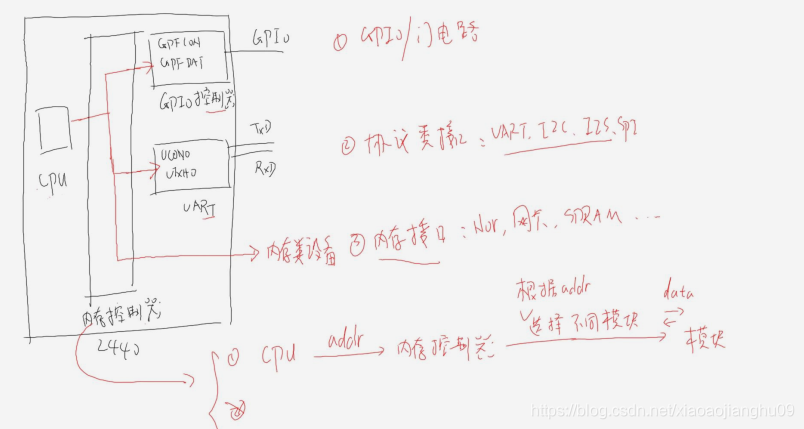
③CPU accesses the memory interface device
CPU and puts the address and data directly on the address bus/data bus of the peripheral device.
Multiple peripheral devices share the address bus and data bus, how can they not interfere with each other?
Each peripheral device has a private CS signal. Different CS signals inside the SOC chip correspond to different banks;
different address areas (banks) correspond to different CSs and are controlled by the memory controller of the SOC chip;
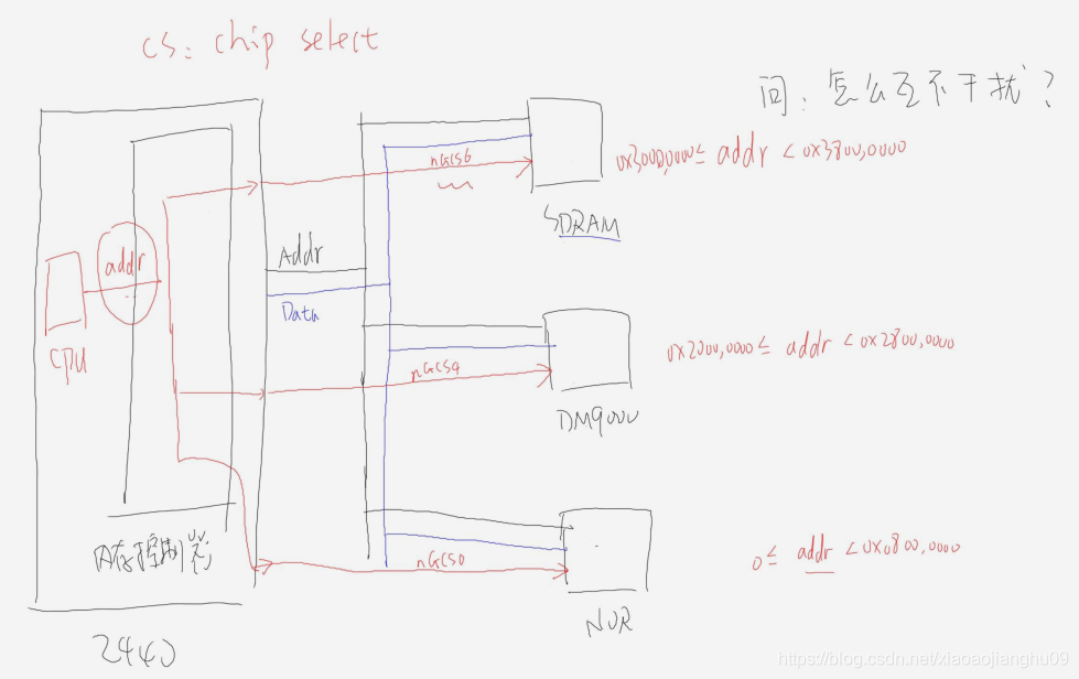
Because the CPU is 32bit, the address sent is also 32bit.
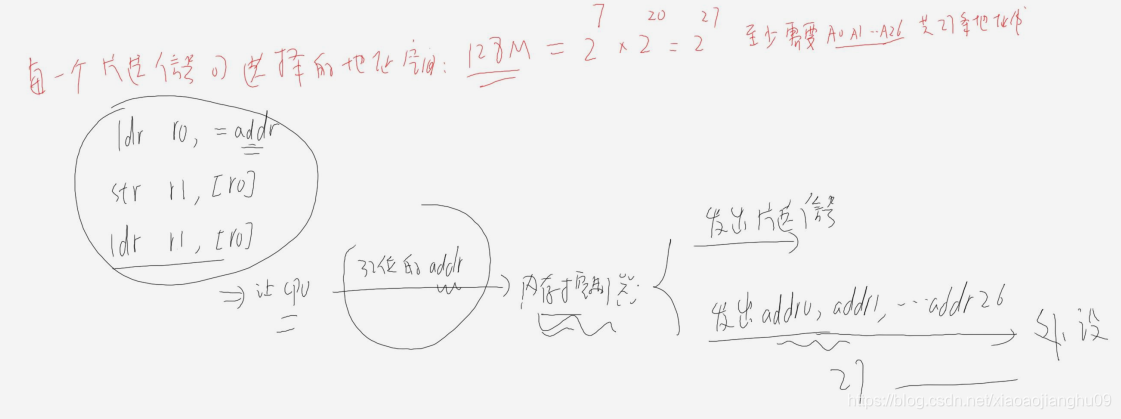
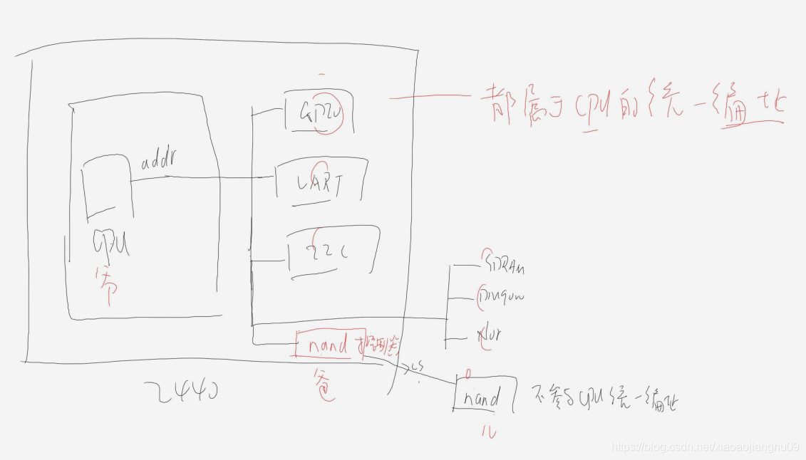
④The particularity of the CPU accessing the nand chip
The address of the peripheral nand device is issued by the nand controller, not directly by the CPU. So nand does not belong to the unified addressing of the CPU.
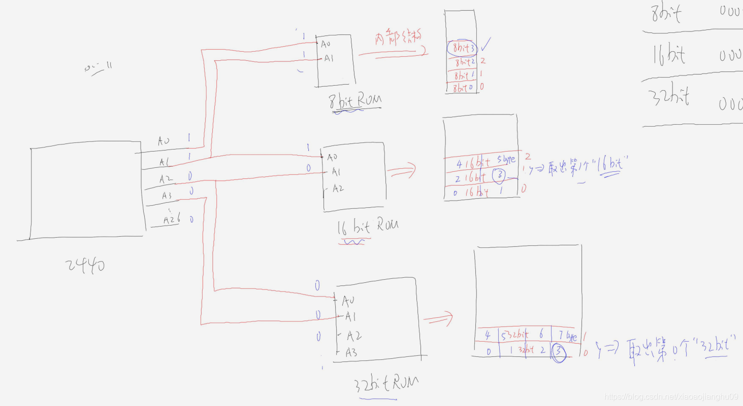
Two different bit width concepts of memory interface
- The address line connection method corresponding to different data line width is different, as follows:
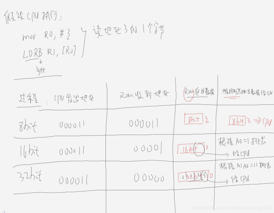
- As shown in the figure below: Suppose the CPU executes the 1byte instruction that reads address 3?
CPU issue address:
A26 A25~A3=0X00
A2 A1 A0=0 1 1
According to the above connection: the address received by different bit width ROM
8bit ROM addr=0x3;//取出第3个的数据
16bit ROM addr=0x1;//取出第1个数据
32bit ROM addr=0x0;//取出第0个数据
After getting the above data, the memory controller picks out the data needed by the CPU!
How to pick it out? Pick out according to the unconnected address line
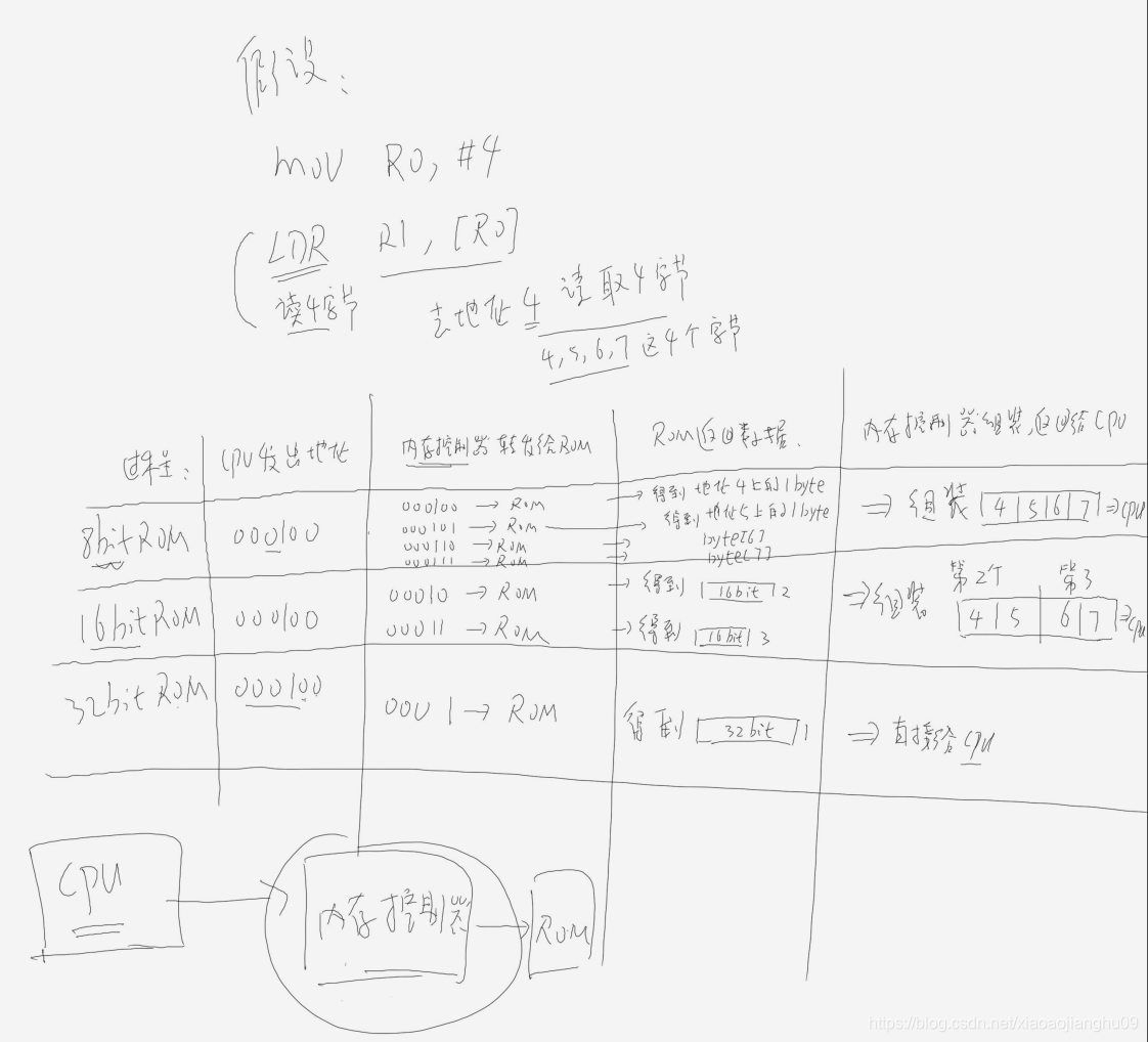
- As shown in the figure below: Suppose you need to read the 4bytes data of address 4?
Because the CPU needs to obtain 4bytes of data, the memory controller sending address and data splicing operations are different for different bit-width ROMs.
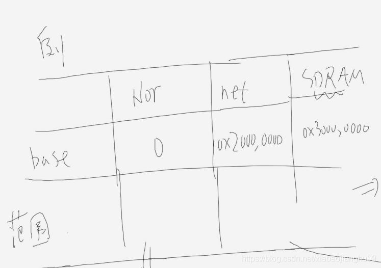
Three-chip access address determination
- Determine the base address according to the chip select signal connected to the chip:
as shown below: NOR NET SDRAM is connected to different CS signals, and different address ranges are obtained according to the chip manual.
- Determine the range according to the address line connected to the chip:
①NOR: use a total of 21 address lines A20~A0
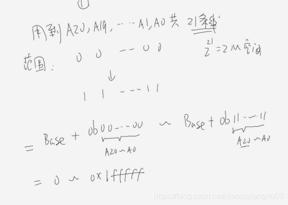
②net: use two address lines A2 and A0

③SDRAM: use 17 address lines

Four-chip access timing diagram
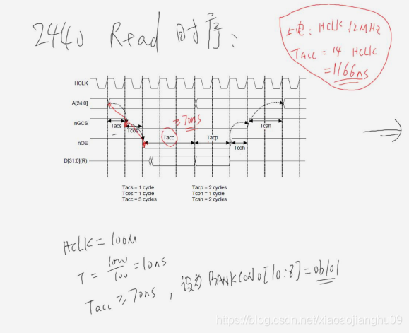
- 2440 read timing diagram
- Timing diagram of a NOR flash
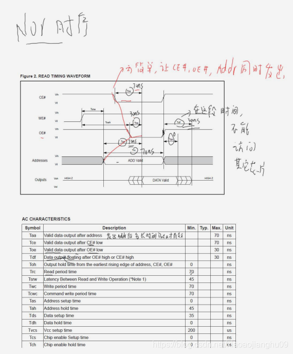
Taa: how long the data is valid after the addr signal is sent
Tce: how long the data is valid after the CE signal is valid
Toe: how long the data is valid after the OE signal is valid
Tdf: after the OE signal or CE signal is invalid, the data line cannot return to high impedance State time
Toh: After the OE signal or CE signal is invalid, the data retention time
Trc: The shortest time of the read cycle