00. Table of Contents
Article Directory
01. Introduction to Random Number Generator
The RNG processor is a random number generator based on continuous analog noise, which provides a 32-bit random number when the host reads.
RNG has passed the FIPS PUB 140-2 (October 10, 2001) test with a success rate of 99%.
02. Main features of random number generator
● Provide 32-bit random numbers generated by the analog generator
● The interval between two consecutive random numbers is 40 PLL48CLK clock signal cycles
● Identify abnormal behaviors by monitoring RNG entropy (generating stable values, or generating stable value sequences)
● Can be banned to reduce power consumption
03. Function description of random number generator

04. Random number generator operation
To run RNG, follow these steps:
-
If necessary, enable interrupts (for this, set the IE bit in the RNG_CR register to 1). An interrupt is generated when a random number is prepared or when an error occurs.
-
Enable random number generation by setting the RNGEN bit in the RNG_CR register to 1. This activates the analog part, RNG_LFSR and error detector.
-
Each time it is interrupted, check to make sure that there is no error (SEIS and CEIS bits in the RNG_SR register should be 0), and the random number is ready (the DRDY bit in the RNG_SR register is 1). Then you can read the contents of the RNG_DR register.
According to the requirements of FIPS PUB (Federal Information Processing Standard Publication) 140-2, the first random number generated after setting the RNGEN bit to 1 should not be used, but it should be saved and compared with the next random number generated. Each random number generated subsequently needs to be compared with the previous random number generated. If any pair of compared numbers are equal, the test fails (continuous random number generator test).
05. Random Number Generator Register
5.1 RNG Control Register (RNG_CR)
RNG control register
offset address: 0x00
Reset value: 0x0000 0000

Bits 31:4 are reserved and must be kept at the reset value.
Bit 3 IE: Interrupt enable
0: RNG interrupt is disabled.
1: Enable RNG interrupt. As long as DRDY=1 or SEIS=1 or CEIS=1 in the RNG_SR register, the interrupt will be suspended.
Bit 2 RNGEN: Random number generator enable (Random number generator enable)
0: Disable the random number generator.
1: Enable random number generator.
Bits 1:0 are reserved and must maintain the reset value
5.2 RNG Status Register (RNG_SR)
RNG status register
offset address: 0x04
Reset value: 0x0000 0000

Bits 31:3 are reserved and must be kept at reset value
Bit 6 SEIS: Seed error interrupt status
This bit is set at the same time as SECS, and is cleared by writing 0 to it.
0: No error sequence
detected 1: One of the following error sequences is detected:
— More than 64 consecutive bits with the same value (0 or 1)
— More than 32 consecutive alternating 0 and 1 (0101010101…01)
if RNG_CR register IE = 1, the interrupt will be suspended.
Bit 5 CEIS: Clock error interrupt status (Clock error interrupt status)
This bit is set at the same time as CECS, and it is cleared by writing 0 to it.
0: PLL48CLK clock
is detected correctly 1: PLL48CLK clock is not detected correctly (f PLL48CLK <f HCLK /16)
If IE = 1 in the RNG_CR register, the interrupt will be suspended.
Bit 4:3 is reserved, must keep the reset value
Bit 2 SECS: Seed error current status
0: No error sequence is currently detected. If the SEIS bit is 1, it means that the error sequence has been detected and normal.
1: One of the following error sequences was detected:
— More than 64 consecutive bits with the same value (0 or 1)
— More than 32 consecutive alternating 0s and 1s (0101010101…01)
Bit 1 CECS: Clock error current status
0: PLL48CLK clock is detected correctly. If the CEIS bit is 1, it means that the clock error has been detected and
normal.
1: The PLL48CLK clock is not detected correctly (f PLL48CLK <f HCLK /16).
Bit 0 DRDY: Data ready
0: RNG_DR register is not yet valid, no random data is available
1: RNG_DR register contains valid random data
Note: If IE = 1 in RNG_CR register, interrupt will be suspended.
After reading the RNG_DR register, this bit returns to 0 until a new effective value is calculated
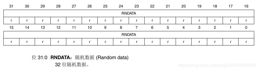
5.3 RNG Data Register (RNG_DR)
RNG data register
offset address: 0x08
reset value: 0x0000 0000
RNG_DR register is a read-only register, and provides a 32-bit random value when read. After reading, this register provides a new random value after up to 40 PLL48CLK clock cycles. Before reading the RNDATA value, the software must check whether the DRDY bit has been set.
5.4 RNG register map

06. Appendix
6.1 [STM32] STM32 series tutorial summary
Website: [STM32] STM32 series tutorial summary
07. Statement
STM32F4xx English Reference Manual