introduction
Sequential logic for digital circuit design is very important, a systematic review article for a portion of the digital sequential logic circuit.
Memory device
Since the timing logic output not only by the influence of the input current, is also affected by the previously input, so the need for a storage unit for storing previously input.
SR Latch (set-reset) --- level sensitive device
Verilog actually in many cases you should avoid using latches should also avoid inadvertently integrated into the latch.
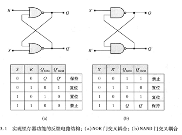
NOR gate cross-coupled latch, while input 11, the output logic is not reciprocal; on the other hand from the logical 11-> 00 initiator competition will result in unpredictable output 11 is avoided;
Su cross-coupled NAND gate access input 00, the output logic is not reciprocal, and initiator competition from 00-> 11, 00 is avoided.
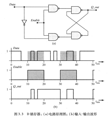
Transparent latch
Also become transparent latch D latch, a belt by increasing the enabled NAND gate circuit, the control input is affecting the output.
D latch is connected to the inverted input terminal of the other, to avoid the prohibited input and output instability
trigger
Edge-sensitive device, the data is synchronized by the operation of an edge of a signal.
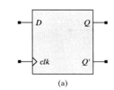
D flip-flop
Master-slave flip-flop
It can be achieved by two transparent latches. When the clock goes low, Data reaches Q1 through the primary latch; when the clock from low to high, the master latch latches, Data through to the output from the latch.
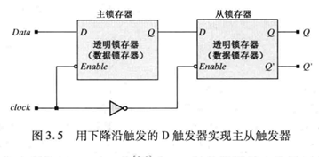
Master slave flip-flop may also be achieved through the transfer gate CMOS process (TG Gate)
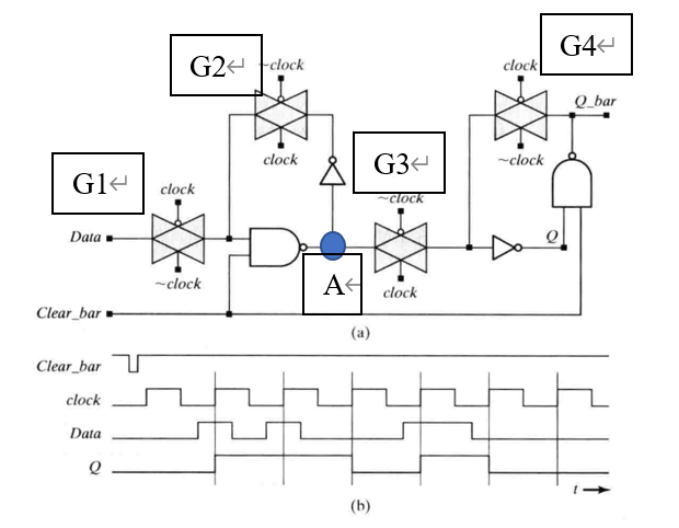
analysis:
1, cleared, A 1 point, Q_bar is 1, Q is 0
2, when the Clock low, opening Gl, G2 off, G3 off, G4 open, Data signal is input to the master latch input. Clock rising edge coming, G1 off, G2 and triggering latch open.
3, G2 G3 simultaneously opened apart, A dot signal through G3, after reaching the negated Q; G4 achieve output latch.
Other triggers
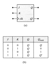
JK flip-flop, 00 maintaining, 11 flip, set the number of 10, 01 is cleared.
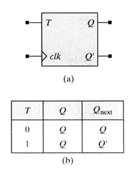
T flip-flops, connected together end JK JK flip-flop, the holding implement input 0, 1 inverted input.
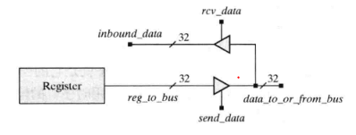
Bus device with tristate
总线:连接系统中多个功能单元多条连线的信号通道。大大减小系统物理资源和板级空间。
三态器件:硬件上实现了总线和电路中的动态接口,使能时作为数据通路,否则开路(Hi-Z)。
三态器件用于电路与总线隔离,如图。send_data为高时,电路向总线输出数据;rcv_data为高时,从总线接收数据。
时序机设计和状态转移图
时序机
时序机的下一步行为或动作由当前输入和当前状态描述。
Mealy状态机下一状态取决于当前输入和当前状态。
Moore状态机下一状态取决于当前输入和当前状态,但输出仅取决与当前状态。
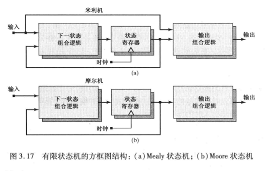
比较
1、Moore机比Mealy机多出一个延迟周期(Mealy机能够对输入进行实时监测),但输入信号的噪声可能对输出的信号产生一定影响。
2、一般来说,Moore型状态机状态多一些。
状态转移图(个人觉得这一部分很关键,但自己也没有十分掌握好,后面通过理解加深逐渐来补充这部分内容吧)
这里以一个例子来说明手工方法来设计状态机的步骤:
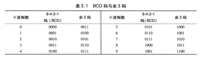
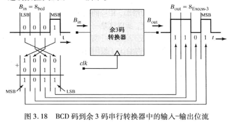
例:BCD码到余3码的转换(余3码是在BCD码的基础上加3,得到的自补码)
在设计时需要注意的是,位流先从最低位输入和输出。
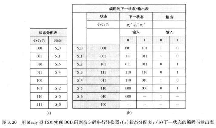
根据表得到状态转移图(这部分自己做的也不够好)。需要列出状态和状态转移关系,合并等价状态,根据以下原则分配对应码字代表状态。
状态编码分配原则:
1、 某个特定的输入,两个状态跳到同一个状态,则分配相邻码字
2、 相邻状态分配相邻码字
3、 某个特定输入,有相同的输出,分配相邻码字

根据状态转移图并分配状态后,得到“当前状态-不同输入下下一状态-不同输入下输出”的表格。
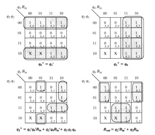
根据上表,分别画出“下q2q1q0Bout的下一状态-q2q1q0qin的当前状态”卡诺图,得到q2q1q0qin的布尔表达式。
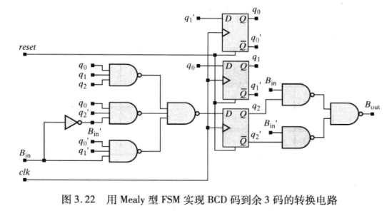
根据卡诺图得到的四个表达式,画出对应的硬件实现。利用三个触发器,分别存储三个状态位。其余利用组合逻辑实现。
状态化简和等价状态
等价状态:时序机两个状态对所有可能的输入都有相同的输出和下一状态(即状态表两个状态有关的行是完全相同的),则称为两个状态等价。
删除并保留仅一个等价状态可使得状态转移图得到化简。但两个状态行不完全相同也可能是等价状态(即需要某些等价消除后才能看出该两个状态行等价)。
总结
本文介绍了数字电路中时序逻辑部分的基础内容,但很大一部分仍需要练习和补充。如果有看客发现错误希望大家能够指出,大家共同进步!