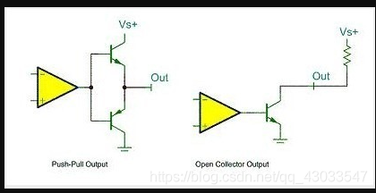
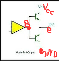
A push-pull output:
can output a high, low , connecting digital devices; generally refers to two push-pull transistors are controlled by two complementary signals, are always in a turned on when the other transistor is turned off. Determined by the high and low power IC.
Two push-pull circuit are the same parameters or the MOSFET transistors, push-pull circuit in the present embodiment, each responsible for the positive and negative half cycle wave amplifying task, operation of the circuit, two symmetrical only one power switch is turned on, Therefore, conduction losses, high efficiency. May be output, the load may draw current from the current sink to the load. Push-pull output stage circuit only improve the load capacity, and increase the switching speed.
When a triode turn off the other, is determined according to terminal B,
which is a comparator if a> 0 B B output; when a <b B output 1

when B is an upper transistor when turned off below;
when B is zero lower transistor is turned on, the top closed.
This push-pull
two, open-drain output:
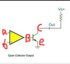
when B is 1, this tube is turned on, OUT is grounded, the output is 0; B is 0 when the tube is not turned on, an output OUT to VCC.
Open drain output: generally only output low , the output of the collector of the transistor to be obtained corresponding to the high level state requires a pullup resistor adapted to do the job type driving current, which is a relatively strong ability to absorb current (. general 20ma or less).
Open drain in the form of circuit has the following features :
-
The drive capability of the external circuit, reduces IC (integrated circuit, also called chips) inside the drive. When the IC internal MOSFET is turned on, a driving current flows from the external VCC R pull-up, MOSFET to GND. IC internal gate only a small drive current.
-
一般来说,开漏是用来连接不同电平的器件,匹配电平用的,因为开漏引脚不连接外部的上拉电阻时,只能输出低电平,如果需要同时具备输出高电平的功能,则需要接上拉电阻,很好的一个优点是通过改变上拉电源的电压,便可以改变传输电平。比如加上上拉电阻就可以提供TTL/CMOS电平输出等。(上拉电阻的阻值决定了逻辑电平转换的沿的速度 。阻值越大,速度越低功耗越小,所以负载电阻的选择要兼顾功耗和速度。)
-
OPEN-DRAIN提供了灵活的输出方式,但是也有其弱点,就是带来上升沿的延时。因为上升沿是通过外接上拉无源电阻对负载充电,所以当电阻选择小时延时就小,但功耗大;反之延时大功耗小。所以如果对延时有要求,则建议用下降沿输出。
-
可以将多个开漏输出的Pin,连接到一条线上。通过一只上拉电阻,在不增加任何器件的情况下,形成“与逻辑”关系。这也是I2C,SMBus等总线判断总线占用状态的原理。补充:什么是“线与”?:
-
在一个结点(线)上, 连接一个上拉电阻到电源 VCC 或 VDD 和 n 个 NPN 或 NMOS 晶体管的集电极 C 或漏极 D, 这些晶体管的发射极 E 或源极 S 都接到地线上, 只要有一个晶体管饱和, 这个结点(线)就被拉到地线电平上. 因为这些晶体管的基极注入电流(NPN)或栅极加上高电平(NMOS),晶体管就会饱和,所以这些基极或栅极对这个结点(线)的关系是或非 NOR 逻辑. 如果这个结点后面加一个反相器, 就是或 OR 逻辑.
其实可以简单的理解为:在所有引脚连在一起时,外接一上拉电阻,如果有一个引脚输出为逻辑0,相当于接地,与之并联的回路“相当于被一根导线短路”,所以外电路逻辑电平便为0,只有都为高电平时,与的结果才为逻辑1。
三、浮空输入
顾名思义就是浮在空中,上面用绳子一拉就上去了,下面用绳子一拉就沉下去了。浮空输入的时候,你想输入大电流都难。浮空输入,内阻比较大,你得很高的电压。
逻辑器件的输入引脚既不接高电平,也不接低电平。由于逻辑器件的内部结构,当它输入引脚悬空时,相当于该引脚接了高电平。一般实际运用时,引脚不建议悬空,易受干扰。
四、上拉输入/下拉输入/模拟输入:
1、上拉输入:上拉就是把电位拉高,比如拉到Vcc。上拉就是将不确定的信号通过一个电阻嵌位在高电平!
2、下拉输入:就是把电压拉低,拉到GND。
3、模拟输入:模拟输入是指传统方式的输入。数字输入是输入PCM数字信号,即0,1的二进制数字信号,通过数模转换,转换成模拟信号,经前级放大进入功率放大器(功率放大器中也是模拟信号)。
五、复用开漏输出、复用推挽输出:
. 可以理解为GPIO口被用作第二功能时的配置情况(即并非作为通用IO口使用)。
最后总结下使用情况:
在 STM32 中选用 IO 模式
(1) 浮空输入_IN_FLOATING ——浮空输入,可以做 KEY 识别, RX1
(2)带上拉输入_IPU——IO 内部上拉电阻输入
(3)带下拉输入_IPD—— IO 内部下拉电阻输入
(4) 模拟输入_AIN ——应用 ADC 模拟输入,或者低功耗下省电
(5)开漏输出_OUT_OD ——IO 输出 0 接 GND, IO 输出 1,悬空,需要外接上拉电阻,才能实现输出
高电平。当输出为 1 时, IO 口的状态由上拉电阻拉高电平,但由于是开漏输出模式,这样 IO 口也就可以
由外部电路改变为低电平或不变。可以读 IO 输入电平变化,实现 C51 的 IO 双向功能
(6)推挽输出_OUT_PP ——IO 输出 0-接 GND, IO 输出 1 -接 VCC,读输入值是未知的
(7)复用功能的推挽输出_AF_PP ——片内外设功能(I2C 的 SCL,SDA)
(8)复用功能的开漏输出_AF_OD——片内外设功能(TX1,MOSI,MISO.SCK.SS)
STM32 设置实例:
(1)模拟 I2C 使用开漏输出_OUT_OD,接上拉电阻,能够正确输出 0 和 1;读值时先
GPIO_SetBits(GPIOB, GPIO_Pin_0);拉高,然后可以读 IO 的值;使用
GPIO_ReadInputDataBit(GPIOB,GPIO_Pin_0);
(2) If the pull-up resistors, IO default is high; IO value needs to be read and to be used and the pull-input floating _IPU input
_IN_FLOATING and open-drain _OUT_OD;
usually 5 ways to use a pin function, they are configured as follows:
1) as an ordinary GPIO input: configure the floating pin is input to the pull-input or input with pull-down belt weak weak, and do not enable
the corresponding pin All alternate-function block.
2) as a common output GPIO: Configure the pin of the push-pull or open-drain outputs, and do not enable the pin corresponding to all replication
functional blocks.
3) as an ordinary analog inputs: the pin is configured as an analog input mode, and do not enable the pin corresponding to all replication functional blocks.
4) as the built-in peripheral input: the required configuration of the floating pin is an input, input pull-up or pull-down with weak input with weak, while enabling the lead
pin corresponding to a multiplexing function module.
5) as built-in peripheral output: Configure the pin is an open drain output of the multiplexing or multiplexing push-pull output, while the enable pin corresponding to the
multiplexing function modules.