Overview:
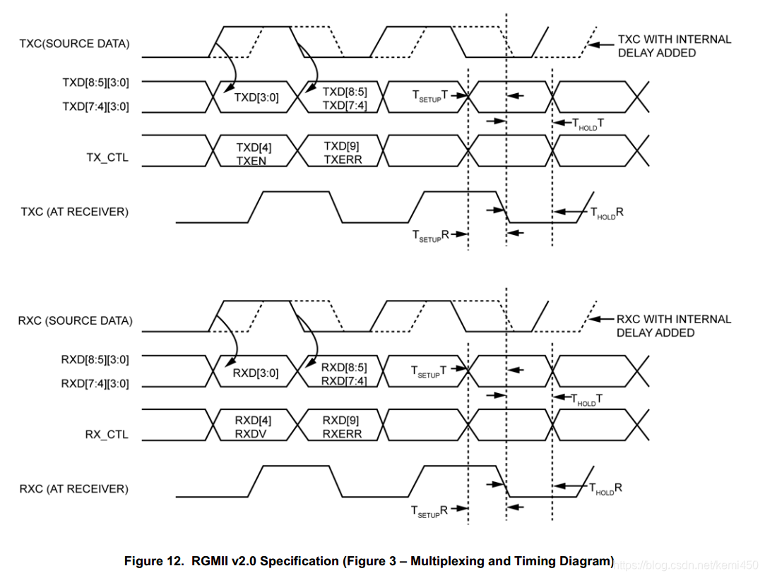
RGMII sequence is double edge sampling clock, RGMII in the default sequence, a clock (RXC / TXC) and the rim edge aligned data (TXD / RXD / TX_CTL / RX_CTL), and therefore, FPGA want to send and receive data correctly, the need for TXC or RXC appropriate delay. Since the highest clock is 125MHz, the optimal delay is 2ns.
Delayed design:
In the third speed network applications, the normal program needs 125MHz, 25MHz and 2.5MHz clock and the clock signal phase shifted by 90 °. And the PLL may not produce the 2.5MHz clock, the program clock number up to six, selector level 2 need not suitable timing constraints. Alternatively, the input clock is a delay, then the internal data processing delayed clock signal, the last clock signal delayed by a certain delay output, to ensure the application of such three-speed network, while a small number of clocks for timing analysis and constraints.
The Xilinx 7z020,7z030 in the series, there IDELAY2 ODELAY2 and accurate clock and data delay, can achieve three-rate applications. Use IDELAY2 and ODELAY2 need IDELAYCTRL a reference clock and 200MHz, and bound into one group. Its use is as follows:
// IDELAYCTRL is needed for calibration
(* IODELAY_GROUP = "rgmii_interface" *)
IDELAYCTRL          idelayctrl_inst
                    (
                    .RDY                (                   ),
                    .REFCLK             (ref_clock_bufg     ),
                    .RST                (idelay_reset       )
                    );

//delay the output clock
defparam            odelay2_inst.CINVCTRL_SEL            = "FALSE"   ;
defparam            odelay2_inst.DELAY_SRC               = "CLKIN"   ;
defparam            odelay2_inst.HIGH_PERFORMANCE_MODE   = "FALSE"   ;
defparam            odelay2_inst.ODELAY_TYPE             = "FIXED"   ;
defparam            odelay2_inst.ODELAY_VALUE            = 25        ;
defparam            odelay2_inst.PIPE_SEL                = "FALSE"   ;
defparam            odelay2_inst.REFCLK_FREQUENCY        = 200.0     ;
defparam            odelay2_inst.SIGNAL_PATTERN          = "CLOCK"   ;
(* IODELAY_GROUP = "rgmii_interface" *)
ODELAYE2            odelay2_inst
                    (
                    .DATAOUT            (clk_out_delay      ),
                    .C                  (1'b0               ),
                    .CE                 (1'b0               ),
                    .INC                (1'b0               ),
                    .ODATAIN            (1'b0               ),
                    .LD                 (idelay_reset       ),
                    .LDPIPEEN           (1'b0               ),
                    .REGRST             (1'b0               ),
                    .CLKIN              (rgmii_clk          ),
                    .CNTVALUEIN         (5'b00000           ),
                    .CNTVALUEOUT        (                   ),
                    .CINVCTRL           (1'b0               )
                    );

// delay the input clock
defparam            idelay2_inst.CINVCTRL_SEL           = "FALSE"     ;
defparam            idelay2_inst.DELAY_SRC              = "IDATAIN"   ;
defparam            idelay2_inst.HIGH_PERFORMANCE_MODE  = "FALSE"     ;
defparam            idelay2_inst.IDELAY_TYPE            = "FIXED"     ;
defparam            idelay2_inst.IDELAY_VALUE           = 25          ;
defparam            idelay2_inst.REFCLK_FREQUENCY       = 200.0       ;
defparam            idelay2_inst.PIPE_SEL               = "FALSE"     ;
defparam            idelay2_inst.SIGNAL_PATTERN         = "CLOCK"     ;
(* IODELAY_GROUP = "rgmii_interface" *)
IDELAYE2            idelay2_inst
                    (
                    .DATAOUT            (clk_in_delay       ),  // Delayed clock
                    .DATAIN             (1'b0               ),  // Data from FPGA logic
                    .C                  (1'b0               ),
                    .CE                 (1'b0               ),
                    .INC                (1'b0               ),
                    .IDATAIN            (clk_in             ),
                    .LD                 (idelay_reset       ),
                    .LDPIPEEN           (1'b0               ),
                    .REGRST             (1'b0               ),
                    .CNTVALUEIN         (5'b00000           ),
                    .CNTVALUEOUT        (                   ),
                    .CINVCTRL           (1'b0               )
                    );
Altera's Cyclone series can be achieved by IOE delay. In the Assignment Editor by Decrease Input Delay or the Increase Delay to Output Pin. Or other Delay.
Since part of the FPGA includes a delay adjustment is not fully functional, therefore, the interface can adjust the internal delay PHY achieve expected results by SMI. Wherein the delay data is a range of -0.42 ~ 0.48ns, the clock delay range is -0.9 ~ 0.96ns.
KSZ9031 the SMI interface program:
// ==============================================================
// RTL generated by Vivado(TM) HLS - High-Level Synthesis from C, C++ and SystemC
// Version: 2016.4
// Copyright (C) 1986-2016 Xilinx, Inc. All Rights Reserved.
//
// ===========================================================

`timescale 1 ns / 1 ps

module smi          (
                    reset                   ,
                    sysclk                  ,
                    start                   ,//start
                    ack                     ,//ack
                    op_mode                 ,//1-read,0-write
                    phy_addr                ,
                    reg_addr                ,
                    write_data              ,
                    read_data               ,
                    read_data_val           ,
                    done                    ,
                    mdc                     ,
                    mdi                     ,
                    mdo                     ,
                    mdoe
                    );
parameter           N = 50_000_000          ;//分频因子,MDC时钟频率=时钟/N;
localparam          Nmax = N-1              ;
localparam          wd = Nmax>0 ? clogb2(Nmax) : 1;

input               reset               ;
input               sysclk              ;
input               start               ;
output              ack                 ;
input               op_mode             ;
input   [2:0]       phy_addr            ;
input   [4:0]       reg_addr            ;
input   [15:0]      write_data          ;
output  [15:0]      read_data           ;
output              read_data_val       ;
output              done                ;
output              mdc                 ;
input               mdi                 ;
output              mdo                 ;
output              mdoe                ;

reg     [15:0]      read_data           ;
reg                 mdoe = 1'b0         ;
reg                 mdo                 ;
reg                 done                ;
reg                 read_data_val       ;
reg                 mdc                 ;
reg                 ack='b0             ;

wire                mdi                 ;
reg [wd-1:0]        sys_cnt ={wd{1'b0}} ;
reg                 clk_en              ;
reg [31:0]          data_reg            ;
reg                 read_flag           ;
reg [ 7:0]          clk_cnt=8'd0        ;

//---0-----1-----2-----
//-start---x-----------
//--------ack----x-----

//clk_cnt[7]:1-work,0-idle
//clk_cnt[0]:mdc

//------------------------SMI timing-------------------------------
// preamble | sof  |  op  | phy |  reg | TA | data | IDLE
//   32x1     01      10   00aaa  rrrrr  z0   16*x    z     (read)
//   32x1     01      01   00aaa  rrrrr  10   16*x    z     (write)
//-----------------------------------------------------------------

//preamble: 128<=clk_cnt<192,
//sof     : 192<=clk_cnt<196,
//op_code : 196<=clk_cnt<200,
//phy addr: 200<=clk_cnt<210,
//reg addr: 210<=clk_cnt<220,
//TA      : 220<=clk_cnt<224,
//data    : 224<=clk_cnt<256,
//IDLE    : 0  <=clk_cnt<127,

//分频产生目标MDC时钟频率
always @ ( posedge sysclk )
    if(sys_cnt == Nmax)
        sys_cnt <= {wd{1'b0}};
    else
        sys_cnt <= sys_cnt + 1;

always @ ( posedge sysclk )
    clk_en <= sys_cnt == Nmax;

//握手信号,开始和应答
always @ ( posedge sysclk )
    if(clk_en)
        begin
            if(clk_cnt==0)
                begin
                    if(start)
                        clk_cnt <= 7'd1;
                end
            else
                clk_cnt <= clk_cnt + 7'd1;
        end

always @ ( posedge sysclk )
    ack <= clk_en & (clk_cnt == 0) & start;

//MDC时钟信号
always @ ( posedge sysclk )
    mdc <= clk_cnt[0] & clk_cnt[7];

//MDIO输出
always @ ( posedge sysclk )
    if(clk_cnt[7]&&clk_cnt<=8'd191)
        mdo <= 1'b1;
    else
        mdo <= data_reg[31];

//MDIO输出使能
always @ ( posedge sysclk )
    if(read_flag)
        mdoe <= (clk_cnt[7] && clk_cnt<=8'd219);
    else
        mdoe <= clk_cnt[7];

//MDIO输入
always @ ( posedge sysclk )
    if(!mdoe & clk_cnt[0] & clk_en)
        read_data <= {read_data,mdi};

//MDIO输入数据完成
always @ ( posedge sysclk )
    read_data_val <= (clk_en&read_flag)&(clk_cnt==8'd254);

//传输完成
always @ ( posedge sysclk )
    done <= clk_en & (clk_cnt==8'd255);

//输出移位寄存器
always @ ( posedge sysclk )
    if(clk_en)
        begin
            if(clk_cnt==0)
                begin
                    if(start)
                        begin
                            data_reg <= {2'b01,op_mode,!op_mode,
                                        2'b00,phy_addr,reg_addr,
                                        2'b10,write_data};
                            read_flag <= op_mode;
                        end
                end
            else if((clk_cnt[7:6]==2'b11)&clk_cnt[0])
                data_reg <= {data_reg,1'b0};
        end

//求log2(xin)
function integer clogb2;
    input integer depth;
        for (clogb2=0; depth>0; clogb2=clogb2+1)
            depth = depth >> 1;
endfunction

endmodule //smi