Article directory
Preface
Recently, communication has been used a lot, including UART, I2C, SPI, DMA, etc. This blog mainly explains the SPI used in recent projects, and combines it with the Puzhong STM32F407ZET6 chip and W25Q128 chip and the corresponding module circuits.
It mainly explains the basic principles and processes of SPI communication, the schematic diagram of W325Q128 and the reading of the chip manual.
1. SPI communication
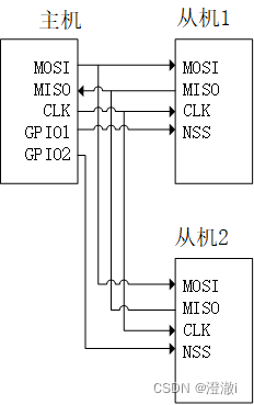
1.1 SPI hardware interface and wiring
SPI communication generally uses four interfaces, which are MOSI,MISO,CLK,NSS
MOSI::master output, slave inputMaster Output Slave Input, master device output/slave device input signal, the signal on the slave device is generally abbreviated as SI. MOSI is the serial data output of the master device, SI is the serial data input of the slave device, and the two signals of the master device and the slave device are connected.
MISO:master input, slave output. Master Input Slave Output, master device input/slave device output signal, the signal on the slave device is generally abbreviated as SO. MISO is the serial data input of the master device, SO is the serial data output of the slave device, and the two signals of the master device and the slave device are linked.
CLK:clock. The clock is given by the master in SPI communication, and the slave does not have CLK.
NSS:Chip Select. In SPI communication, in the case of one master and multiple slaves, generally speaking, only when the chip select pin is set low, the corresponding slave is valid. Some chips are active high.
The connection diagram for one master and multiple slaves is roughly as follows:
1.2 SPI transmission protocol
SPI communication performs serial transmission driven by CLK. The SPI transmission protocol defines the SPI start signal, end signal, data validity, and clock synchronization.
The data frame length of each SPI transmission is 8 bits or 16 bits.
There are four timing modes for SPI communication. The four timing modes are related to the two parameters CPOL and CPHA. The former is clock polarity (Clock Polarity), and the latter is clock phase (Clock Phase).
CPOL:Clock polarity. The level when the clock is in idle state. If CPOL=0, CLK is low level when idle; if CPOL=1, CLK is high level when idle.
CPHA:clock phase. If CPHA=0, the data is sampled on the first edge of SCK; if CPHA-1, the data is sampled on the second edge of SCK.
All four timing modes can be seen in the following table:
| Timing mode | CPOL | WASH | illustrate |
|---|---|---|---|
| 0 | 0 | 0 | The clock idle is low, and the first transition edge data of SCK is sampled. |
| 1 | 0 | 1 | The clock idle is low, and the second transition edge data of SCK is sampled. |
| 2 | 1 | 0 | The clock idle is high, and the first transition edge data of SCK is sampled. |
| 3 | 1 | 1 | The clock idle is high, and the second transition edge data of SCK is sampled. |
The figure below shows the timing diagram corresponding to CPHA=0, CPOL=1 and CPOL=0. If you understand this, you should know the principle of SPI.
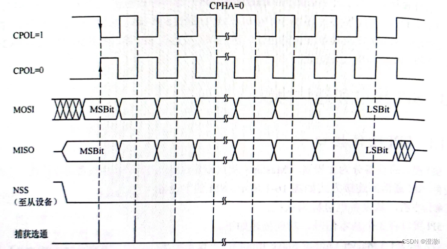
Pay special attention when using SPI communication.The SPI timing of the master and slave devices must be consistent.In fact, this is similar to the master-slave data analysis method. If my master transmits in timing mode 0 and the slave receives in timing mode 3, then the data received by the slave will be inconsistent with the data sent by the master. Pay special attention to this.
1.3 SPI data transmission
There are three ways to transmit data through SPI: blocking, interrupt and DMA.
Let’s briefly introduce each one separately. This blog will use the simplest blocking sending for verification.
1. Blocking type.
Generally, the function used in blocking type sending is: HAL_SPI_Transmit(), this function means blocking type sending data in a buffer.
The complete definition is as follows:
HAL_StatusTypeDef HAL_SPI_Transmit(SPI_HandleTypeDef *hspi, uint8_t *pData, uint16_t Size, uint32_t Timeout)
Generally, the function used for blocking reception is: HAL_SPI_Receive(), this function means blocking reception of data of a specified length and saving it to the buffer.
The complete definition is as follows:
HAL_StatusTypeDef HAL_SPI_Receive(SPI_HandleTypeDef *hspi, uint8_t *pData, uint16_t Size, uint32_t Timeout)
The meaning of the four formal parameters of the sending and receiving functions:
hspiIt is the SPI peripheral object pointer, indicating which SPI pointer is used.
pDataThe pointer representing the sent/received data buffer
Sizeindicates the length of the sent/received buffer data
Timeoutand indicates the timeout waiting time. The unit is the number of system tick signal beats. By default, it is ms.
In addition to the separate sending and receiving functions above, there is also an integrated sending and receiving function HAL_SPI_TransmitReceive(). This function represents a blocking method of sending and receiving data of a certain length at the same time.
The complete definition is as follows:
HAL_StatusTypeDef HAL_SPI_TransmitReceive(SPI_HandleTypeDef *hspi, uint8_t *pTxData, uint8_t *pRxData, uint16_t Size,uint32_t Timeout)
The meanings of several parameters of this function are similar to the above, but the pointers for sending and receiving data are separated, that is, a sending and receiving pointer is turned into a sending pointer and a receiving pointer.
Divide pData into pTxData and pRxData. I will not explain other parameters here.
2. Interrupt
type Corresponding to the blocking type above, there are three functions for interrupt type sending and receiving data. They are: HAL_SPI_Transmit_IT(), , HAL_SPI_Receive_IT()and HAL_SPI_TransmitReceive_IT()
the complete definition is as follows:
HAL_StatusTypeDef HAL_SPI_Transmit_IT(SPI_HandleTypeDef *hspi, uint8_t *pData, uint16_t Size)
HAL_StatusTypeDef HAL_SPI_Receive_IT(SPI_HandleTypeDef *hspi, uint8_t *pData, uint16_t Size)
HAL_StatusTypeDef HAL_SPI_TransmitReceive_IT(SPI_HandleTypeDef *hspi, uint8_t *pTxData, uint8_t *pRxData, uint16_t Size)
We compare blocking sending and find that their parameters are actually the same, except that there is a timeout parameter missing. So I won’t explain the common parts. The difference is that there is an IT after the function name, which means Interrupt.
These three functions all represent sending/receiving data in an interrupt manner, and interrupt events will be generated after their execution is completed.
The interrupt sending mode will generate SPI_IT_TXE, and the callback function will be called: HAL_SPI_TxCpltCallback()
The interrupt receiving mode will generate SPI_IT_RXNE, and the callback function will be called: HAL_SPI_RxCpltCallback()
The interrupt sending and receiving mode will generate SPI_IT_TXE, SPI_IT_RXNE, and the callback function will be called:HAL_SPI_TxRxCpltCallback()
Regarding callback functions and the like, it is actually similar to my blog on external interrupts , and will not be elaborated here.
3. DMA type
DMA has three functions for sending and receiving data,
they are: HAL_SPI_Transmit_DMA(), HAL_SPI_Receive_DMA(), and HAL_SPI_TransmitReceive_DMA()
the complete definition is as follows:
HAL_StatusTypeDef HAL_SPI_Transmit_DMA(SPI_HandleTypeDef *hspi, uint8_t *pData, uint16_t Size)
HAL_StatusTypeDef HAL_SPI_Receive_DMA(SPI_HandleTypeDef *hspi, uint8_t *pData, uint16_t Size)
HAL_StatusTypeDef HAL_SPI_TransmitReceive_DMA(SPI_HandleTypeDef *hspi, uint8_t *pTxData, uint8_t *pRxData, uint16_t Size)
DMA will also generate interrupts, but there are two types of interrupts, namely transfer complete and transfer half-complete.
| DMA mode function | function function | DMA stream interrupt event | Corresponding callback function |
|---|---|---|---|
| HAL_SPI_Transmit_DMA | Send data in DMA mode | DMA transfer completed/DMA transfer half completed | HAL_SPI_TxCpltCallback()/HAL_SPI_TxHalfCpltCallback() |
| HAL_SPI_Receive_DMA | Send data in DMA mode | DMA transfer completed/DMA transfer half completed | HAL_SPI_TxCpltCallback()/HAL_SPI_TxHalfCpltCallback() |
| HAL_SPI_TransmitReceive_DMA | Send/receive data in DMA mode | DMA transfer completed/DMA transfer half completed | HAL_SPI_TxRxCpltCallback()/HAL_SPI_TxRxHalfCpltCallback() |
2. W25Q128
I have seen many STM32 development boards, and they all use this chip as an example chip for SPI communication. The basic configuration and principles of SPI communication are not difficult. When I first started learning, I found it difficult. It is very likely that you need to read the chip manual to communicate with the chip you are using. In this section, I will write about using the chip for SPI communication. Read the detailed chip manual. I'll write an article and post it later.
2.1 Film Selection
Our SPI has data transmission pins, clocks, and chip selects.
Generally, the signal chip select signal is pulled low to be valid. This can be seen from the introduction in the chip manual and the timing diagram.
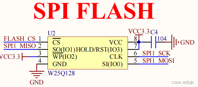
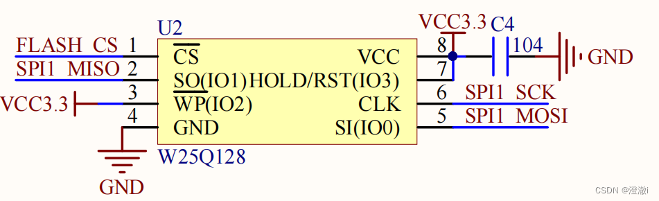
The picture below is the schematic diagram of the W25Q128 part of the Puzhong F407ZET6 development board. We can see that the chip select/CS is active at low level. There is a bar mark on it, which means it is active at low level.
The following is a basic introduction to chip selection taken from the chip manual.
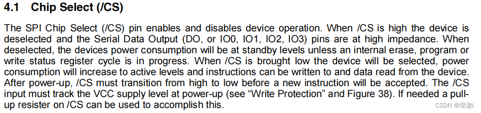
Translate the key part in human words:
/CS is pulled high, indicating that the device is not selected and the serial output pin is in a high-impedance state. When unselected, the chip is in standby mode and does nothing except internal erase, program, or write status register cycles.
/CS is pulled low and the device is selected. When the chip is activated, programmers can write control instructions and data into it.
To put it bluntly, pulling low is effective, but pulling high is ineffective.
2.2 Control instructions
The purpose of this blog is to obtain the device ID, so we need to find out how to obtain the device ID after confirming that the chip select is low.
Check the data sheet and find part of the information in the figure below.
This table tells us that we use Command instruction 90h, which means inputting the control word 0x90h to the chip. The following dummydoes not mean stupid. In the electronics industry, this means a dummy, that is, an invalid unit, just to fill in or meet certain requirements or For constraints, we usually just give 00h.
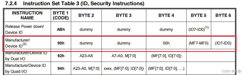
Here is a reminder. After we give the command to obtain the device ID, it will continue to be sent until the chip select is pulled high.
As I write this, it is actually still a bit foggy. Why does the chip send me ID data when I send this command? How do I know when the chip is sent and when I send the data? This has something to do with the timing diagram. Now let’s analyze the timing diagram.
2.3 Timing diagram analysis
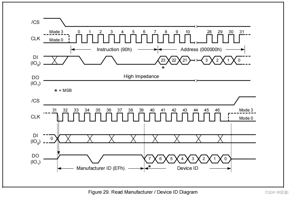
The above picture is connected, but it is layered due to the width of the page. In order to facilitate viewing, I have slightly organized the screenshots so that it looks more complete.
What we have here is SPI communication. First look at the chip select, then look at the clock to determine the mode, and then look at the data transmission direction.
First of all, the film selection is lowered. We can see that the data transmission part will only occur when the chip select is pulled low. Once it is pulled high, all subsequent data transmission will exist. This shows that the film selection is effective in pulling down the price (I have said it many times, which is a bit verbose)
Next look at the clock. In this timing diagram, CLK has Mode3 and Mode0 modes, and the corresponding CPOL and CPHA are both 0 and 1. The specific corresponding relationship has just been written down, if you forget it, please refer to it. The master and slave in this mode must be consistent. Here W25Q128 only supports mode 0 and mode 3, so its clock effect is listed in the timing diagram of the chip manual.
We can see that the first 8 clock cycles are the control instruction cycle, and the following cycle from the ninth cycle (the number is 8, starting from 0) to the 32nd cycle is the write address cycle. The subsequent clock cycles until /CS is pulled high actually have nothing to do with the host input. The timing diagram DI is followed by XXX, which is invalid data.
Let’s look at data transmission again. When the host inputs instructions to the chip, we look at the DI line and see that the data is valid and the DO line is in a high-impedance state. Combined with the clock, the host data is valid in the first 32 clock cycles and invalid after that. At the beginning of the 33 clock cycle, the data in DI becomes XXXX, which is invalid. At this time, the data on the DO line is valid, indicating that the chip is sending data to the host. And keep sending until the chip select pulls high.
The continuous transmission of data here is actually introduced in the chip manual, xxxx can be read continuously.
At the same time, if our address is partially 01, the output is first the device ID and then the manufacturer ID, so we won’t discuss it too much here.

3. STM32CubeMX configuration
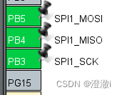
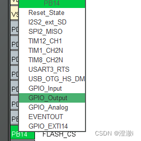
3.1 Pin configuration
Take a look at the wiring diagram


Combined with the schematic diagram, we configure it.
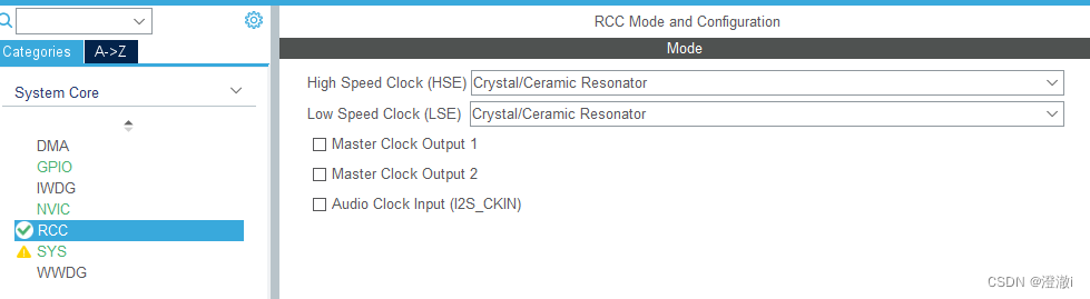
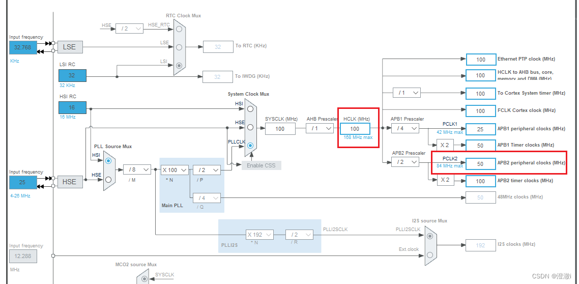
3.2 Clock configuration
Turn on the external crystal oscillator. I have written before that this does not have to be turned on. As long as the frequency you want meets the required requirements and can be obtained by frequency division of the internal crystal oscillator, you do not need to turn on the external crystal oscillator. I usually turn it on habitually, and it won't affect anything.
 SPI1 is on the APB2 bus, so the baud rate of SPI communication is actually calculated based on the frequency of PCLK2.
3.3 SPI configuration
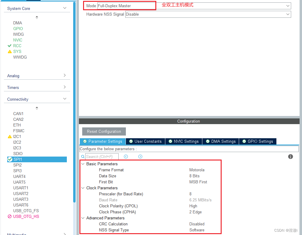
Explain the meaning of this field:
Mode:working mode. When STM32 is used as the host, it generally selects the full-duplex host and the slave full-duplex slave. Full duplex means that MISO and MOSI lines can be used to receive and send at the same time. There is also half-duplex mode, which uses only one data line to send and receive, but can only have one function at the same time.
Hardware NSS Signal:Hardware NSS signal. There are three options. Disable means not using NSS hardware signal; Hardware Nss Input Signal means hardware NSS input signal. Select this option when the SPI slave uses hardware NSS signal. Hardware Nss output Signal indicates the hardware NSS output signal. Select this when the SPI host outputs chip select. However, we use a separate GPIO as the slave chip select signal, so it is set to Disable here.
Frame Format:Frame format. There are two options: Motorola and TI. But generally only Motorola can be selected. This parameter corresponds to the FRF bit of the control register SPI_CR2.
Data Size:Data size. The number of bits in the data frame, optional 8/16bits.
First Bit:Bits preferred for transmission. Optional MSB First or LSB First.
Prescaler(for Baud Rate):Prescaler coefficient used to generate the baud rate. Just take the bus frequency of APBx corresponding to that SPI and divide it by this frequency division coefficient, which is the baud rate. This is APB2, so it is 50MHz divided by 8, so the baud rate is 6.25MBits/s.
I won’t explain CPOL and CPHA, I’ve already talked about them at the beginning.
CRC Calculation:CRC (Cyclic Redundancy Check). This is mainly the CRC calculation result of one byte added to the end of the transmitted data. When a CRC error occurs, an interrupt can be generated. If not used, it defaults to the Disabled
NSS Signal Type:NSS signal type. This parameter is determined by the selection result of Hardware NSS Signal above. When Hardware NSS Signal is disabled, the option of this parameter can only be Software, which means that software is used to generate the NSS output signal, that is, this example uses the PB14 output signal as the chip select signal of the slave.
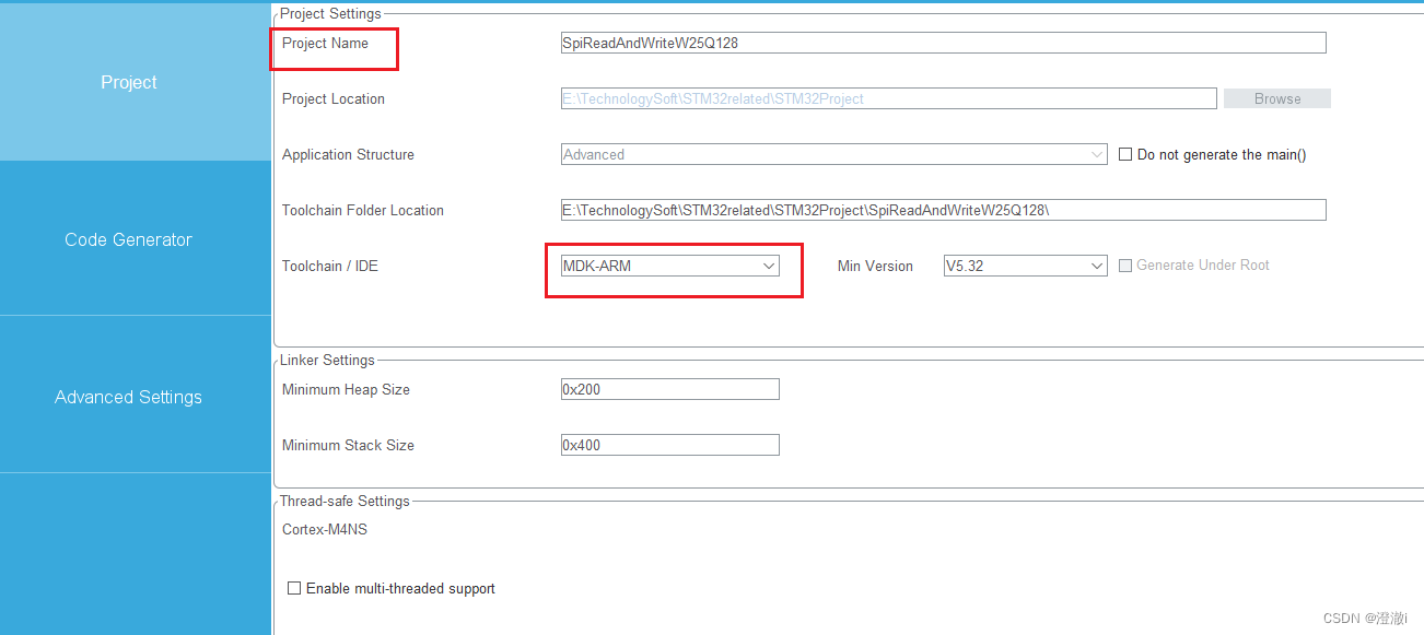
3.4 Project configuration
Project configuration varies from person to person, here is a reference
4. Code writing
4.1 Read ID function
Post the code first, then explain in detail.
uint16_t Flash_ReadIDbywzy(void)
{
	uint16_t Temp = 0;
	uint8_t	byteData=0;
	uint8_t commandData=0x90;
	HAL_GPIO_WritePin(FLASH_CS_GPIO_Port, FLASH_CS_Pin, GPIO_PIN_RESET);//cs=0
	HAL_SPI_Transmit(&hspi1, &commandData, 1, 200);
	commandData=0x00;
	HAL_SPI_Transmit(&hspi1, &commandData, 1, 200);
	HAL_SPI_Transmit(&hspi1, &commandData, 1, 200);
	HAL_SPI_Transmit(&hspi1, &commandData, 1, 200);

	HAL_SPI_Receive(&hspi1, &byteData, 1, 200);
	Temp=byteData;
	Temp=Temp<<8;//Manufacturer ID

	HAL_SPI_Receive(&hspi1, &byteData, 1, 200);
	Temp|=byteData;	//Device ID

	HAL_GPIO_WritePin(FLASH_CS_GPIO_Port, FLASH_CS_Pin, GPIO_PIN_SET);

	return Temp;
}
The flow of the code:
first define some variables for receiving and sending data, then the SPI communication process, enable chip select, and send instructions. What is sent here is 0x90000000. Then start reading data, one byte of data at a time, read twice, read After completing the data, pull the chip select high to end a transmission and return the received data.
For code verification, if you don't have any tools at hand (such as USB to TTL, screen, etc.), then break off the debugging and look at the data.
When the breakpoint reaches the third one, you can see it by looking at the flashID variable. The first two digits are the Manufacturer ID, and the last two digits are the Device ID.
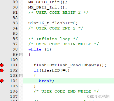
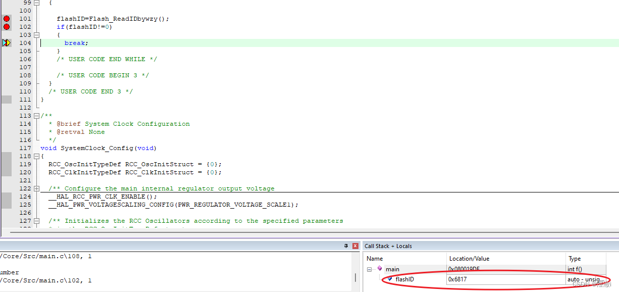 There may be some bugs in the single-step debugging here. After executing break for the first time, the value of the flashID is FFFF. Then press RST and then run to the break point of break, and it will have the correct ID.
The core code is posted here, and there are some details that I won’t write here, such as defining functions, adding header files, burning configurations, etc. The repetitive things have been written before, so I won’t go into details here. It’s the same thing. There is no point in writing more.
I uploaded the complete code and project engineering to the resources corresponding to the blog. Pick up if needed.
Summarize
This blog covers everything from SPI communication principles to W25Q128 chip manual reading, timing diagram reading, to STM32CubeMX configuration and code writing. The entire project is very complete and forms a closed loop. The writing is also very detailed. I don’t know whether it is popular or not, but I think it is quite easy to understand.
This blog was indeed very time-consuming to write, but fortunately it was very rewarding.