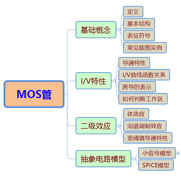
This article has five parts
1. Preface - Why do you need to understand MOS tubes
2. The basic concept of MOS tube
3. I/V characteristics of MOS tube
4. Secondary effect of MOS tube
5. Abstract circuit model of MOS tube
(It takes about 10 minutes to read the full text, and the content is not rigorous or even ridiculed. Let’s take a look at the picture for fun and deepen your impression. If you read some parts of this article, there is a sense of ambiguity that is unclear , it must be that the blogger himself didn’t understand it, and started paddling, so I hope you will come down and read the book to review more professional knowledge. Of course, in the end, I hope that the content of this issue will be beneficial to you)
foreword
It is said that wine is a gut-piercing medicine, and color is a bone-scraping knife, so in modern electronic systems, our MOS tube brother is the Italian cannon of traditional vacuum tube electronics and separated solid-state radio frequency circuits , and is gradually using his unparalleled Performance, ultra-low power consumption, and extremely small size have blasted traditional craft circuits into the history museum , and of course are constantly improving everyone's awareness of integrated circuits.
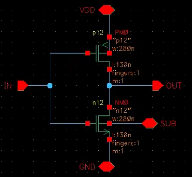
This issue mainly introduces the basics of MOS tubes . We know that Cascode and Gilbert units are the most common circuit structures in RF microwave circuits (often used in LNA, PA, Mixer, VGA, PS and other circuits), so before talking about these slightly complicated circuit structures, Let's take a look at a simplified circuit below. You can stop and think about it:
Problem introduction: As shown in the figure below, assuming Vth0=0.7V, ignoring the channel modulation effect and body effect (ie lambda=0, gama=0), analyze the circuit in the figure below, when Vx changes from 0V to 3V, Ix is What about a response curve, and how does the M1 tube work? ? ?

(Tips: Big guys can discuss the results in three situations ((0, 1); (1, 1.2); (1.2, 3)). If you have any questions, you can add the Xiaobian friend of Microwave Radio Frequency Network and join the group discussion , there is the editor’s WeChat QR code at the end of the article)
Well, let’s get down to business, the main purpose of this blog post is: I hope to summarize the basic knowledge of MOS tubes, 1: Give students a study outline; 2: Give students who are interviewing for jobs a convenient way to consult; 3: Also I hope that the content of this issue can give practitioners a small library of reviewing the past and learning the new. Therefore, the following will be expanded as follows:
basic concept
1) Definition
MOS tube is the abbreviation of MOSFET (Metal-Oxide-Semiconductor Field-Effect Transistor, MOSFET). MOSFET is a metal-oxide semiconductor field effect transistor. Of course, we usually call it a MOS tube. In order to make NMOS and PMOS together, CMOS (Complementary Metal Oxide Semiconductor) is more commonly used.
After reading the passage above, you guys are still confused, what are you talking about, brother throwing bricks? ? ? I know all the Chinese characters you wrote, but why my brain still doesn't know what you are talking about! ! !
Little brother/little sister, don’t worry, let’s read on——
2) Structure
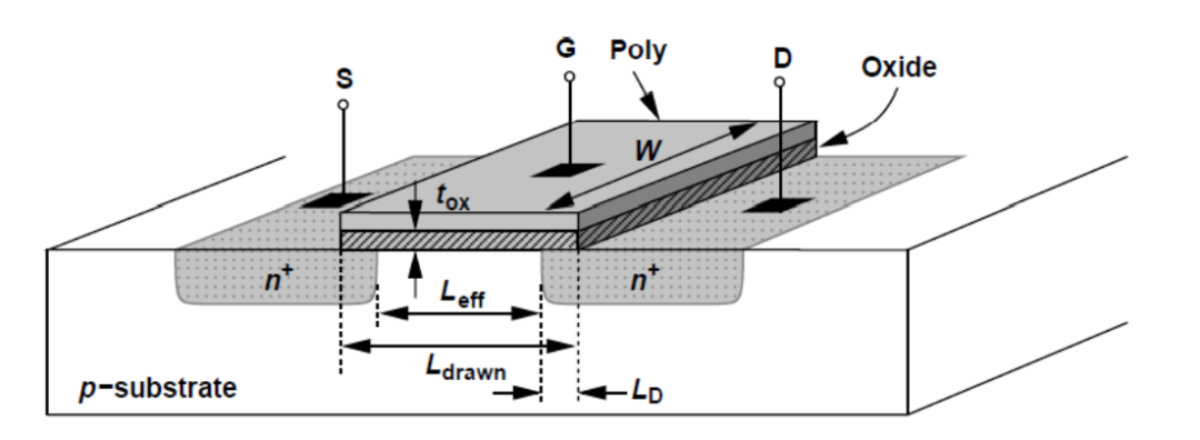
MOS tubes are divided into NMOS and PMOS. Let’s put aside all kinds of complicated technological processes, let’s take a look at the true face of NMOS, as shown below:
First of all, we need to understand why we need to do MOS. In fact, simply speaking, we need a device that can make a big difference with a small size, and use a small voltage to achieve the output of a large voltage swing (that is, the amplification effect. Of course, it can also be used. It is to control whether there is an output, that is, it can also be used as a switch).
Well, since the MOS tube is used as a control (small and large) device, there must be such a triangular relationship: A and B are the initiator and receiver, and C is the regulator, just like the one above A small tube gave An Deming two glasses of water.
In the actual process, we have seen the NMOS structure mentioned above, where D and S are the initiator and receiver. We usually call D the drain and S the source (of course it is just called that, in a certain Under certain specific voltages, the identities of the two brothers are interchangeable), and then G we call it the grid (that is, the middleman, you can also call it a pimp with a small and broad), and the pimp G grid is for To avoid one day the incident will happen. When working, you will use a thin layer of insulating oxide film to isolate yourself from D and S, that is, the oxide on it has a thickness of tox. Then the distance between D and S, that is, the equivalent gate length, we call the equivalent channel length Leff of the MOS tube . Even more frightening, he plans to mass-produce the distance between D and S to 1.4nm in 2027 , what, what about in China? Well, I don’t know, everyone can leave a message to discuss)
By the way, what is the full Chinese name of the MOS tube? Oh, metal-oxide semiconductor field effect transistors , then here we have introduced the structure of field effect transistors based on metal D, S, G and oxide films, and then the so-called semiconductors naturally mean our gates G, Drain D, source S, and the office of the oxide film, of course, their office did not just choose a site for fun, they chose the P substrate with low doping concentration as the site, in order not to cause bad things , The site and the so-called G, D, and S try not to have an office romance, at least not to affect the work of G, D, and S. Therefore, the so-called low doping of the P substrate in NMOS means that it is basically non-conductive under normal circumstances. It is just to provide the function of the venue (of course, it is said that long-term love, our substrate sometimes has some feelings and influences on the MOS tube, we will continue to talk about this in the secondary effect of the MOS tube later evil fate).
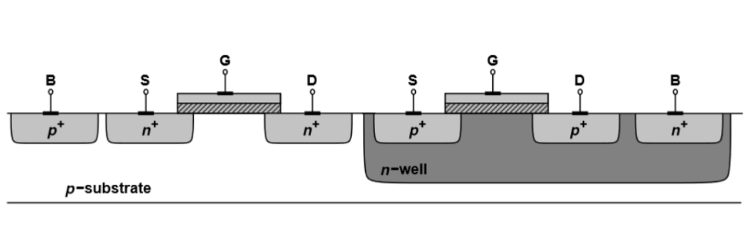
Well, above we have roughly understood the basic composition of the function of the MOS tube. In actual use, we generally use the complementary metal oxide half field effect transistor process, which is the famous CMOS process. Its structure is shown in the figure below:
Everyone will definitely say that the city has deep routines, and I want to go back to the countryside. It’s not like our family has no land. Why do you feel wronged and squeeze yourself together to work?
What I want to say is that it is not enough for a young man to just have land at home. After all, it is 2022 AD, and modern society emphasizes efficiency and win-win cooperation! So when we put NMOS and PMOS together, we can often achieve twice the result with half the effort, but then again, the businesses they operate are a bit different. The prerequisites for NMOS and PMOS to form a channel need potential. The change of the barrier voltage, so naturally speaking, the type of doping is a bit different. It seems that although everyone is doing business in the mall, but still need to make some compartments to distinguish their respective functions, then in CMOS In the process, an N-Well is made on the P substrate, and then PMOS can be built into this N-WELL, so that PMOS and NMOS can play together happily.
3) Indicates the symbol
In order to make the communication process smoother, our physicists and engineers have defined some symbols for NMOS and PMOS, which are like our traditional Chinese pictographs, as shown in the figure below:
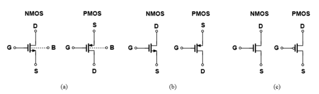
In (a), (b), and (c) are the pictographic symbols of NMOS and PMOS. You can use them according to your own preferences. Generally speaking, we will connect the terminal voltage (B, Bulk) of the substrate to ground Or on VDD, so (b) and (c) are used more often, and the symbolic expression of (c) is used more in digital circuits (indicating switches).
4) Common layout examples
I believe that when you are interviewing, many interviewers often ask you to draw the cross -sectional diagram of the most typical inverter in order to check whether you understand the structure of NMOS and PMOS tubes clearly . The cross-sectional view of PMOS still needs to be understood a lot. Here is a schematic diagram and layout (not a cross-sectional diagram) of a classic inverter for your reference.
Well, after talking about the basic concept of MOS tubes, let’s enter a little bit of mathematics (don’t be intimidated, in fact, these mathematical formulas are also a way of expressing physical phenomena, just like the pictograph symbols we mentioned above , he makes our expression more refined, so in this blog post we don’t do mathematical derivation, we only do porters of nature), then let’s discuss below, how does this MOS tube work! ! !
I/V characteristics of MOS tube
As mentioned earlier, our study of I/V characteristics is not for derivation, but for us to understand the working status of MOS tubes more clearly, which can be more concise and refined in subsequent expressions, so we focus on the discussion of MOS tubes in this part. Working status (mainly discussing NMOS tubes, PMOS is actually an extra minus sign in many cases, you can analyze it yourself), and how to judge the working status, and draw the I/V characteristics in each status according to the mathematical formula.
1) Conduction characteristics

As shown in the figure above, when we keep increasing VG, what will happen? ? ? We can see that the gate and the substrate will be equivalent to a capacitive plate, then the VG voltage increases, and the charge accumulated on the gate metal plate begins to increase. When the charge is large enough to form a channel, the At this time, D and S will be turned on. At this time, our VG is the so-called " threshold voltage ", VTH voltage. We then continue to increase VG, and at this time the charge density in the channel continues to increase, resulting in a further increase in the drain-source current. Well, then the VTH we just mentioned is a qualitative analysis. Below I will directly give the calculation formula of VTH in semiconductor physics:
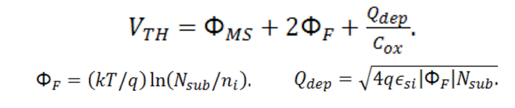
in

is the voltage value of the difference between the work function of the polysilicon gate and the substrate, where Nsub is the doping concentration of the substrate, q is the electronic charge, ni is the intrinsic carrier concentration of silicon, and Qdep is the charge in the depletion region, Cox is the gate oxide capacitance per unit area.
Of course, it is impossible for us to use the above mathematical formula for actual calculation, because these parameters, I am afraid that ordinary people will not be able to test them. How do we get VTH? Next, let me explain the IV characteristic function in detail. Of course, the current major technology manufacturers generally have a VTH0 in the SPICE parameter, which we can use directly.
2) I/V curve function relationship

First of all, we still assume that VG is added to the gate of the NMOS transistor, the source S is grounded, and a VD voltage is added to the drain, and then according to the following formula (it doesn’t matter if you don’t understand it, you can go to the group or add the author’s friend to leave a message to discuss):
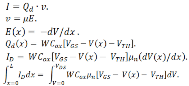
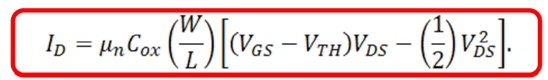
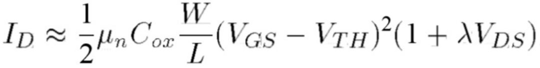
Well, regardless of the derivation process, we can directly get the mathematical function expression of the NMOS drain current ID:
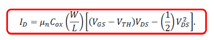
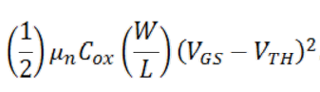
That is to say, at this time our current is related to the carrier mobility, capacitance per unit length, VGS, VTH and VDS (parabolic equation), we find a partial derivative of ID with respect to VD and make it 0, this You can see that you want the ID to get the maximum value, and the ID is:
Bingo, I believe that everyone who has studied analog circuits has a little impression of the value of ID and max at this time, haha, it is the current when the NMOS tube is saturated, that is to say, when VD=VGS-VTH , the current of our NMOS tube will tend to be stable, that is, it will reach saturation (we will discuss this later).
Here we need to talk about the two parameters in the above formula separately:
1 is our VGS-VTH, which is the famous "overdrive voltage". How to say it, in order to understand it vividly, we can turn on when our VG just reaches VTH, but we continue to add voltage (that is, VG-VTH is still There is more food), at this time, the drive is flying, so we understand that there is nothing wrong with the drive voltage (haha, let’s understand it this way first, in fact, this statement is still a bit worth studying).
2 is our W/L, which is the "width-to-length ratio" we mentioned in our daily work. In the above formula, the maximum output current of the entire MOS tube can be changed by adjusting the width-to-length ratio. In the follow-up blog post, we The effect of aspect ratio on transconductance, noise, linearity, etc. will also be discussed.
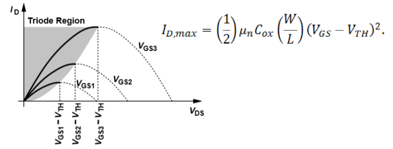
Well, so far we have probably discussed three current and voltage states [haha, are you thinking in your heart at this time : what, what? Where did the three come from? Bro, you didn’t lie to me, did you? I only saw one type, which is the VDS=VGS-VTH you mentioned. My God, am I dazzled? 】 Okay, let's turn the time back to the beginning of this section:
1. When VG is less than VTH, our tube is cut off at this time, which is what we call the cut-off area, and the current is 0;
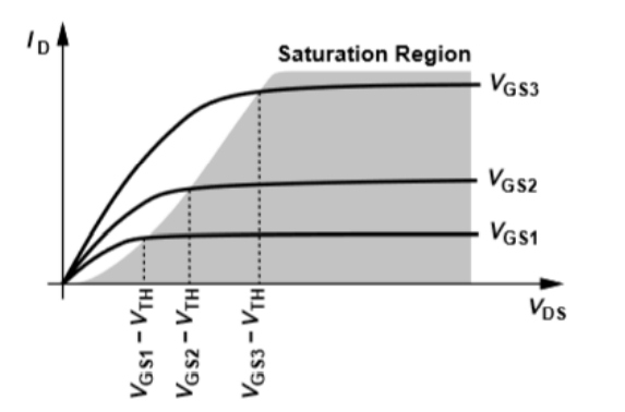
2. When VG is greater than VTH, and VDS≥VGS-VTH, the tube is in the saturation region at this time, and the current is:
3. When VG is greater than VTH, and VDS<VGS-VTH, it is a triode region (also called a linear region), and the current is
Well, that’s all, let’s experience it for ourselves (maybe it’s still a bit convoluted, it’s okay, we will have an easier way to determine which area we work in later)
3) Expression of transconductance
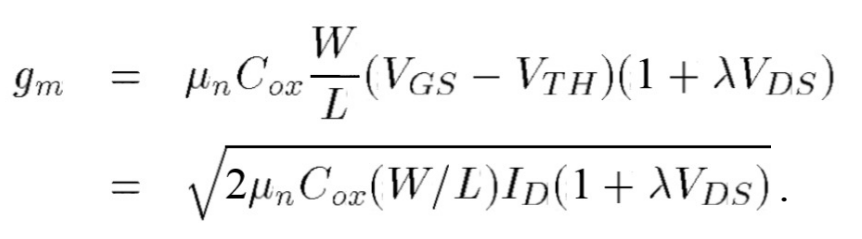
This part of the content, just be lazy, do not go into details of its basic origin, directly according to the above current formula for a partial differential of the input voltage, that is, when the tube is in the saturation region:
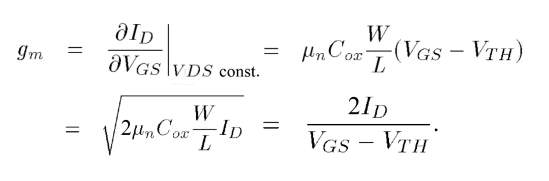
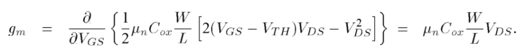
When the tube is in the triode region (linear region):
Through the size of the transconductance, we can know the ability of the tube to dial four ounces. That is to say, if VGS slightly changes the ID of our door, there will be a large change. gm is the value to measure the ability of four ounces .
4) How to quickly judge the working status of the NMOS tube
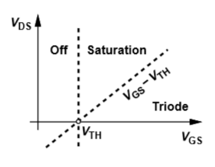
Here we take over the part of the working area for judging the NMOS tube. From the above figure, we can know:
1. Let's look at the abscissa. When VGS is less than VTH, that is, to the left of the vertical dotted line, the tube is cut off and is in the cut-off area ;
2. When VGS is greater than VTH on the horizontal axis, the oblique dotted line is VD=VGS-VTH, and above the oblique dotted line is VDS greater than VGS-VTH, and the tube is in saturation, that is, the saturation zone ;
3. Continue to look at the horizontal axis when VGS is greater than VTH, the oblique dotted line is VD=VGS-VTH, and below the oblique dotted line is VDS less than VGS-VTH, and the tube is in Triode, that is, the triode area or the linear area ;
Well, now everyone should be clear about the distinguishing conditions of each work area, so let’s add a concept, that is, when our MOS is used for switching, what state is it in when it is turned on? What is the turn-on resistance at this time? Well, let’s go down to find the answer to this question or discuss it in the group.
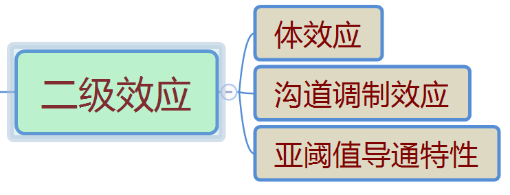
Secondary effect of MOS tube
When it comes to the secondary effect of the MOS tube, in fact, it is mainly the bad edge between the substrate and the source, the channel length effect and the subthreshold conduction characteristic that we talked about before.
1) Body effect
When it comes to body effect, we used to default that the substrate terminal is connected to GND, that is to say, we consider the value of VSB as a fixed value by default, then VTH can be obtained according to the previous formula, BUT, we know When VB becomes more negative (or the relative value of VSB becomes more negative), then more holes will be attracted to the substrate electrode, leaving a large amount of charge, making the depletion layer wider
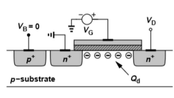
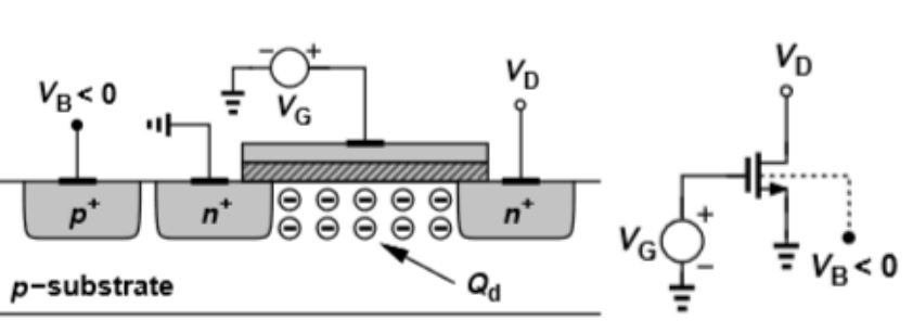
Therefore, the new calculation formula of the threshold voltage VTH affected by the receptor effect at this time is expressed as follows:
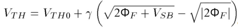
VTH0 is the previous threshold voltage. Generally, our process manufacturers will give this value in the SPICE file, and VSB is the voltage difference between the source of the MOS transistor and the substrate.
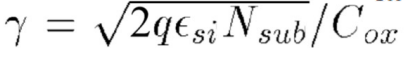
It is the body effect coefficient. Similarly, generally our process manufacturers will give this value in the SPICE file, and we can directly bring it in when we calculate.
2) Channel modulation effect
This effect occurs in the saturation region , as shown in the figure below, the local charge density of the inversion layer is proportional to VGS-VTH-V(x), so when V(x) is close to VGS-VTH, the charge density drops to 0, that is, the reverse The type layer is terminated at this time, and we increase the voltage difference between the drain voltage and the source voltage, so that the inversion layer will come earlier than the first snow in 2002. In other words, with the gap between the gate and the drain When the voltage difference increases , the actual inversion channel length gradually decreases (haha, here also indirectly shows that the channel modulation effect is not in the cut-off region and the triode region)
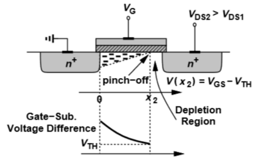
Lambda is the communication modulation modulation coefficient. Of course, in actual engineering, this value will be given in the SPICE parameter of the MOS tube. In the same way, we can find the transconductance under the channel modulation effect according to the new ID:
3) Subthreshold conduction characteristics
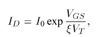
This feature is a bit anti-three, because we have been talking about it before, when VGS is less than VTH (that is, the gate-source voltage is less than the threshold voltage), the tube is turned off, but the reality is the survival desire of our MOS tube brother Very strong, when VGS is approximately equal to VTH or slightly less than VTH, there is still a weak inversion layer, and there are some small drain-source currents, then maybe the big guy will ask again, this small waywardness of the MOS tube and What will it bring?
When I was in middle school and high school, I wrote small English essays by heart. The most classic is "Every coin has two sides". Then the sub-threshold conduction characteristics of MOS tubes are the same. It will lead to a small current in the tube. Once this current accumulates, it will be a rather terrifying existence. For example, when millions or even hundreds of millions of tubes are working, this small current will be a terrible power consumption; On the other hand, when our MOS tube is in the sub-threshold region, the current has an exponential relationship with VGS, and a larger gain can be obtained at this time:
How do we transition to the sub-threshold region for normal MOS transistors that usually work in the triode region or saturation region? The answer is that when keeping ID unchanged and increasing the gate width W, VGS is gradually approached or even slightly smaller than VTH, or we reduce the current ID, then one result is that the speed of the sub-threshold circuit is very limited.
Abstract circuit model of MOS tube
1) Small signal model of MOS tube
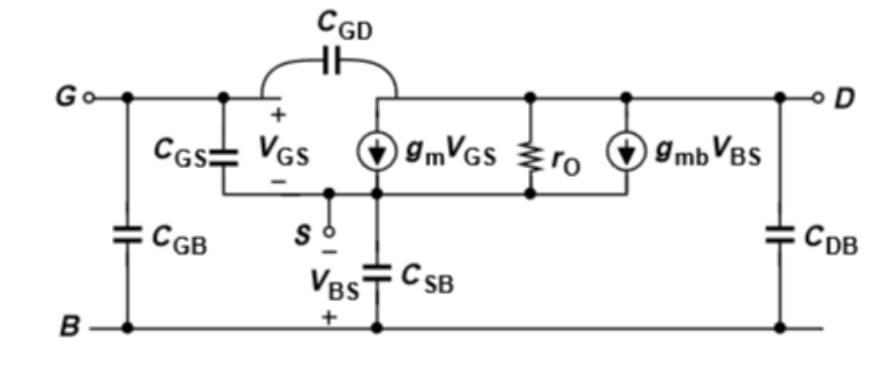
Before analyzing the small signal model of the MOS tube, we must first understand why it takes so much time to do this. First of all, as mentioned earlier, we use MOS tubes mainly to make switches or to control the amplification effect of four or two dials. Then with this premise, do we have to follow this goal to analyze the relationship between voltage and current? ? Well, since we are going to do such a thing, we will find a way to create a model, and then use our simple KVL/KCL rules to analyze it, and finally we get how to use the "four twos" to toggle . "Jianjin", in other words, we build a small signal model to derive the mathematical expression of the relationship between the output and input of the MOS tube. The small signal model of the common NMOS is first given below, and then we will gradually disassemble its composition:
How to get the small signal model of the MOS tube above?
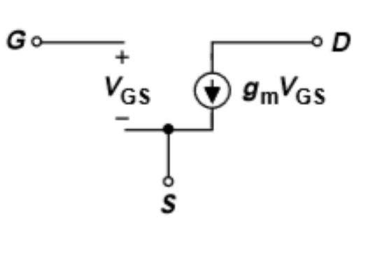
First of all , for MOS tubes, we add a voltage variable at the gate-source terminal, and then we can detect the corresponding current change at the drain terminal, that is to say, the MOS tube can use a voltage-controlled current source connected between the source and drain. To simulate changes, the following basic model is obtained:
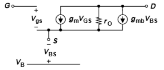
Then , we take into account the channel modulation effect in the secondary effect, that is to say, our ID will have an additional factor analyzed above, and we divide it by the voltage, which can be equivalent to a resistance ro:

Therefore, the small signal model at this time can be changed to this:

Then , we take the body effect in the secondary effect into account. Similarly, according to the above analysis, our ID will have a change about VTH, that is, there will be a relative VSB between the gate and source. The voltage source exists, and then the controlled source will have one more gmb*VSB when seeking current at the drain. Therefore, the small signal model at this time continues to become:
Finally , we take into account the capacitive effect of the MOS tube, that is to say, we will talk about it when we analyze the conduction characteristics. There will be some channels inside the MOS tube, which can be equivalent to capacitance, so we can simply get the following figure:

Therefore, we bring it into the above small signal model considering the secondary effect of the MOS tube, and finally we get the small signal model of the MOS tube as follows:

So, how to use this small signal model to analyze IV curve or transconductance characteristics? You can disassemble it by yourself, or if the feedback in this issue is not bad, and everyone is actively liking and reposting, then we can find a time to publish another issue later to analyze how the signal propagates in the model.
2) SPICE model of MOS tube
In fact, the SPICE model, like the small signal model above, is a generalist in describing circuit characteristics.
After years of hard work by our scientists (mainly professors from UCB University) and engineers, we have found a set of procedural description language for describing the working state of the tube - SPICE model. SPICE is the abbreviation of Simulation Program with Integrated Circuit Emphasis. It is a powerful general-purpose analog circuit simulator that describes the actual electrical connection inside the device. In the circuit analysis program of integrated circuits, Spice's netlist format has become the standard for the description of ordinary analog circuits and transistor-level circuits. Its first version was completed in 1972 and written in Fortran language. The official practical version was launched in 1975. , was designated as the National Industrial Standard of the United States in 1988, and is mainly used for the design and simulation of electronic systems such as ICs, analog circuits, digital-analog hybrid circuits, and power circuits.
Ok, so what exactly is a SPICE model? Can you be more specific, haha, let’s not make a fuss, this article will carry a "LEVEL1" SPICE model of 0.5um CMOS process :
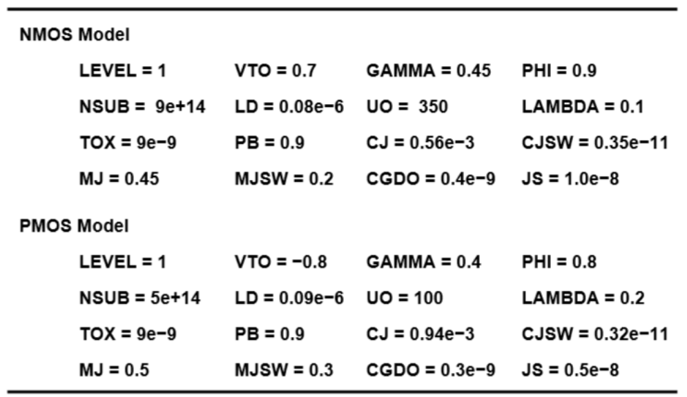
Have you ever been surprised, why is there only one form? Haha, yes, it is actually a table, and the relationship between each grid is established through a programming language. So what do you think of this? as follows:
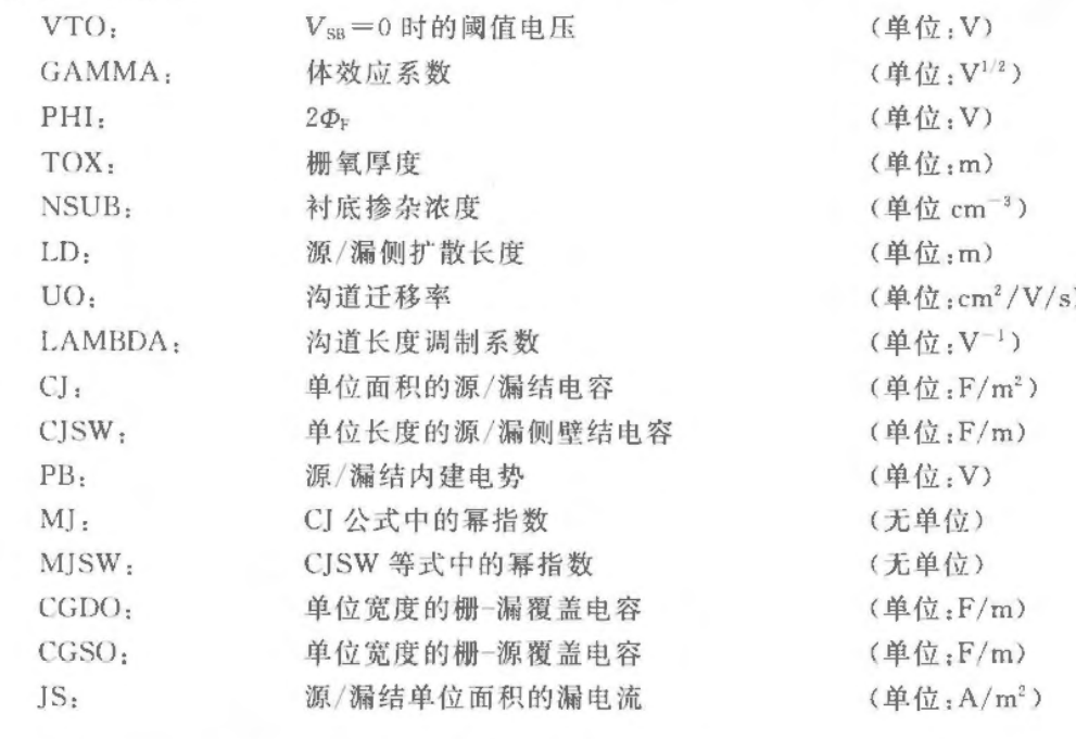
Of course, there are some models that describe MOS tubes, such as IBIS model, Verilog-AMS model and VHDL-AMS model, etc. We will not tell them one by one. Of course, the most important thing is that I don’t know much about it.