Article Directory
====>>> Article summary (with code summary) <<<====
1. Preparations
1.1. Hardware preparation
This chapter will use two different ways to drive the LCD screen.
The first type: FSMC interface
The development board used: Puzhong-Zhunrui-Z100 STM32F103 development board, the main control is STM32F103ZET6.
The second type: software simulation 8080 communication protocol
Development board used: punctual atom Mini development board, main control STM32F103RCT6.
Display screen used: punctual atomic 2.8-inch TFTLCD screen.
- Size: 2.8 inches;
- Resolution: 320×240;
- 16-bit true color display;
- Interface: 16-bit 8080 bus;
- Comes with a touch screen.
1.2. 8080 bus
The 8080 parallel interface was invented by INTEL and is widely used in various liquid crystal displays.
The interface can choose 8-bit or 16-bit data line communication.
If you choose 8-bit data line communication, you need the following signal lines, a total of 13 lines:
- CS: OLED chip select signal;
- WR: write data to OLED;
- RD: read data from OLED;
- D[7: 0]: 8-bit bidirectional data line;
- RST(RES): hard reset OLED;
- DC: command/data flag (0, read and write commands; 1, read and write data).
If you choose 16-bit data line communication, you need the following signal lines, a total of 21 lines:
- CS: TFTLCD chip select signal;
- WR: write data to TFTLCD;
- RD: read data from TFTLCD;
- D[15:0]: 16-bit bidirectional data line;
- RST: hard reset TFTLCD;
- RS: command/data flag (0, read and write commands; 1, read and write data).
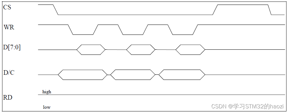
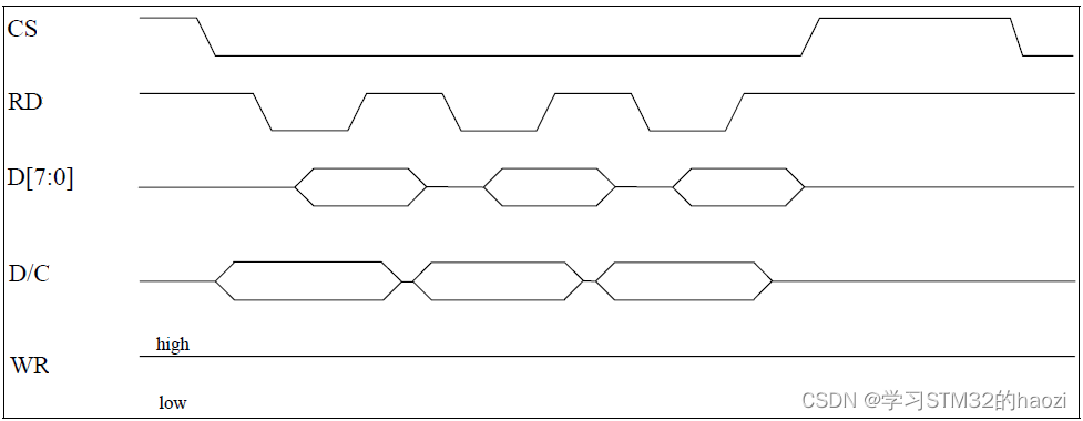
8080 parallel port read/write process is:
- Pull down the chip select CS to select the storage device;
- Set DC/RS high (data)/low (command) according to the type of data to be written/read;
- Then we set RD/WR low according to whether to read data or write data;
- On the rising edge of RD, the data is latched onto the data line (D[7:0])/D[15:0];
- On the rising edge of WR, the data is written into the storage device;
Timing diagram (8 bits and 16 are the same except for the number of data bits)
8080 parallel port write timing diagram
8080 parallel port read timing diagram
Not difficult.
1.3. TFT_LCD
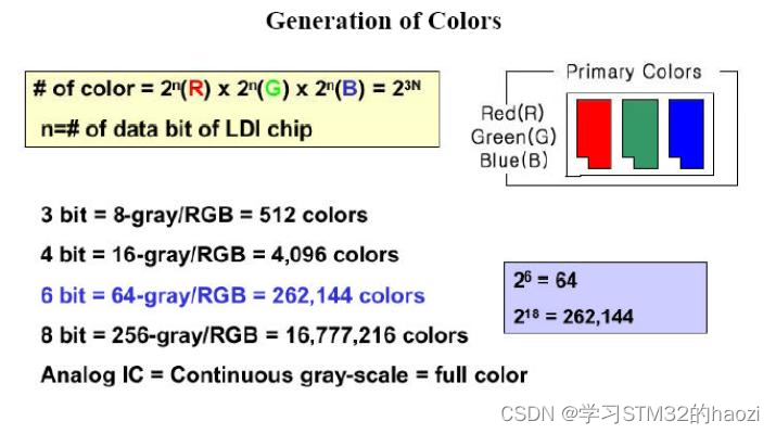
The memory chip used in the LCD here is ILI9341 liquid crystal controller, with its own video memory, and the total size of the video memory is 172800 bytes (240 * 320 * 18 / 8).
- 320*240 corresponds to the screen resolution on the screen;
- 18 means 18-bit mode, RGB 3 colors are 6 bits respectively, each color is 64 gray scales, and then the free combination of three colors is 260,000 colors, that is to say, each pixel can have 260,000 colors;
- 8 means that the previous unit is bit, and / 8 is followed by byte.
But in fact, we use 16位the mode, in this mode, ILI9341 uses RGB565the format to store color data, at this time, the corresponding relationship between the 18-bit data line of ILI9341, the 16-bit data line of MCU and LCD GRAM is shown in the figure:
| 9341 bus | D17 | D16 | D15 | Q14 | D13 | D12 | D11 | D10 | D9 | D8 | D7 | D6 | D5 | D4 | D3 | D2 | D1 | D0 |
| MCU data line (16 bits) | D15 | Q14 | D13 | D12 | D11 | NC | D10 | D9 | D8 | D7 | D6 | D5 | D4 | D3 | D2 | D1 | D0 | NC |
| LCD GRAM (16 bits) | R[4] | R[3] | R[2] | R[1] | R[0] | NC | G[5] | G[4] | G[3] | G[2] | G[1] | G[0] | B[4] | B[3] | B[2] | B[1] | B[0] | NC |
It can be seen that for the ILI9341 chip, the useful data lines are: D17-D13 and D11-D1. However, after drawing out the useful 16 data lines, they can just correspond to D0-D15.
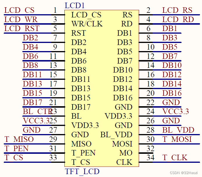
Then look at the schematic diagram of the LCD module.
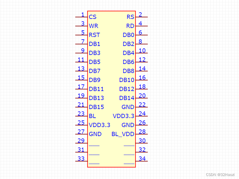
Regardless of the internal structure of the module, just look at the lead-out pins (labels in the middle of the red box), the bottom 29-34 pins are related to the touch screen, let’s ignore it here:
- Pins 1-4 are the corresponding signal control lines;
- Pin 5 is the reset line, which is connected to the reset button of the development board;
- Pins 6-21, that is, D0-D15 in the middle of the red box, are 16 data lines for communication;
- The remaining ones that stick out are relatively short are VCC and GND;
- The 23rd pin BL and the 28th pin BL_VDD are used to provide backlight for the LCD.
BL_VDD is the power input. The BL input voltage determines the brightness. It can be controlled by PWM, or it can be directly input high level to pull it up.
Note: The label in the middle of the box here is marked with the data bits of the MCU in the above table. It can be mapped to the ILI9341 chip according to the above table.
Simply speaking , the 8080 communication interface is used. If the RESET line is not counted, a total of 21 lines are needed. Other internal principles are not important.
Instructions (simply read a few, just understand the meaning, don’t need to delve into it, I can’t remember many of them):
- Command 1: 0XD3, used to read the ID of the LCD controller.
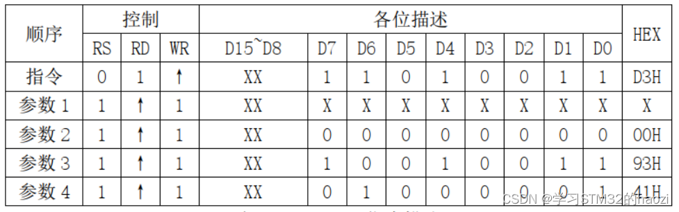
- Instruction 2: 0X36, this is the storage access control instruction, which can control the reading and writing direction of the ILI9341 memory. Simply put, when writing GRAM continuously, it can control the growth direction of the GRAM pointer, thereby controlling the display mode (the same is true for reading GRAM ).
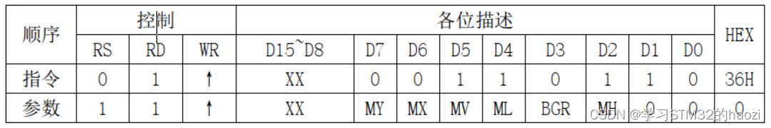
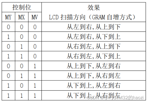
After the 0X36 instruction, there is a parameter. Here we mainly pay attention to: MY, MX, MV these three bits, through the setting of these three bits, we can control all scanning directions of the entire ILI9341.
Just these few first, as long as you know there are, you can check the chip manual for details.
1.4. FSMC
FSMC (Flexible Static Memory Controller, Variable Static Memory Controller) : It is a new type of memory expansion technology adopted by the STM32 series . Capable of interfacing with synchronous or asynchronous memory and 16-bit PC memory cards. It has unique advantages in external memory expansion, and can easily expand different types of large-capacity static memory according to the application needs of the system.
Generally, chips with more than 100 pins will have FSMC interface.
FSMC block diagram
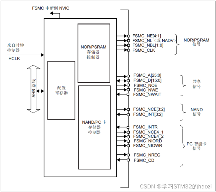
It can be seen that the FSMC of STM32 divides external devices into 3 categories:
- NOR/PSRAM devices;
- NAND devices;
- PC card device.
They share signals such as the address data bus, and they have different CSs to distinguish different devices. TFTLCD can also be controlled as SRAM to realize the effect of LCD display.
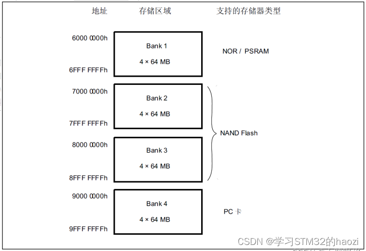
The FSMC of STM32 divides the external memory into four memory blocks with a fixed size of 256M bytes, with a total of 1G.
2. Create a project
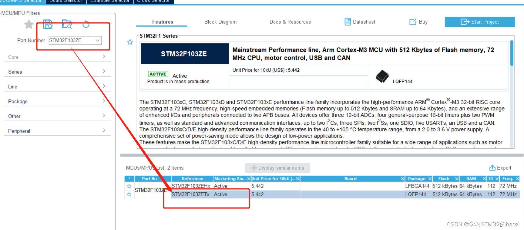
2.1. Select master
Just select the corresponding master controller on the development board.
- If you use the punctual atom Mini development board, choose STM32F103RCT6;
- If you use a common development board, choose STM32F103ZET6.
ZET6 has FSMC interface, which can be driven by FSMC, and the software can simulate 8080 interface (but why bother).
If RCT6 does not have FSMC interface, it can only use software to simulate 8080 interface.
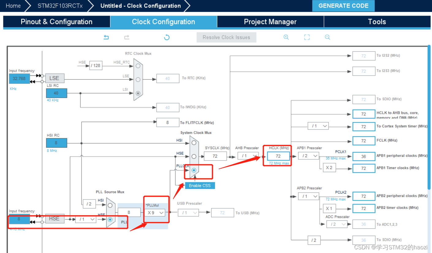
2.2. System configuration
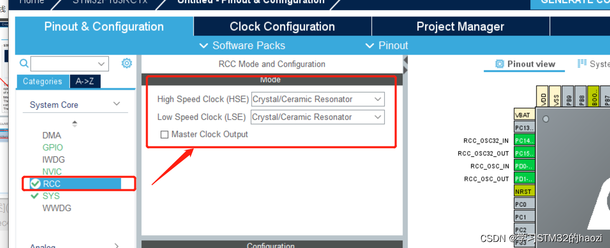
Configure the clock source
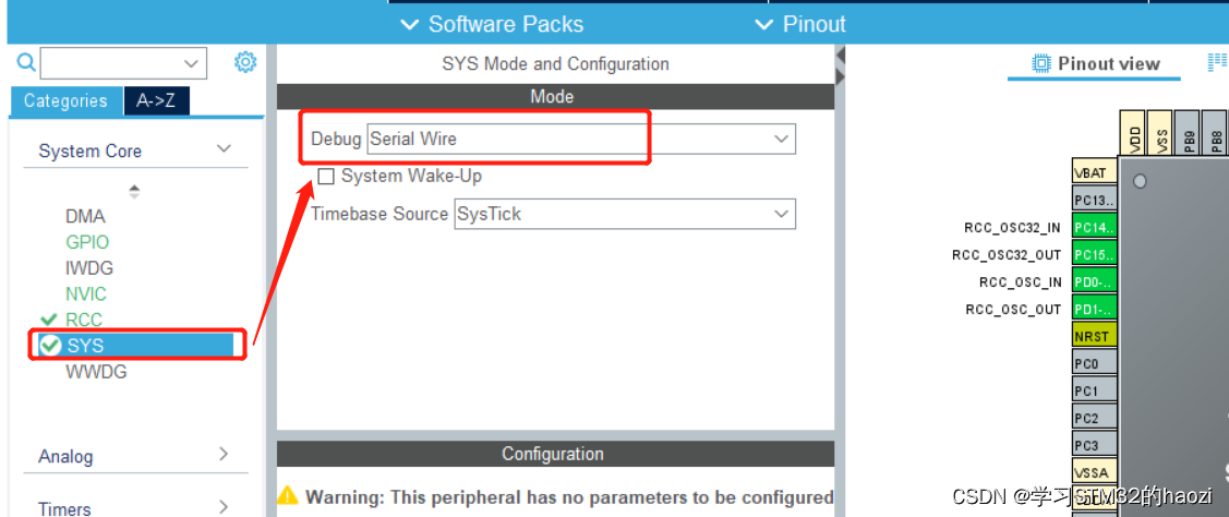
Configure the debug mode (you can check it if you need ST-Link download and debug)
Configure the clock tree (you can directly enter 72 in HCLK, and then press Enter to automatically configure)
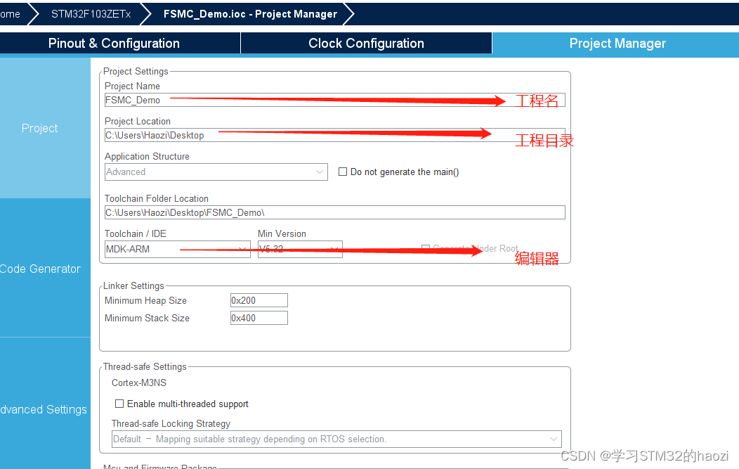
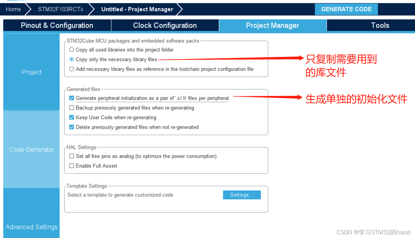
2.3. Configuration project directory
3. FSMC drive LCD
3.1. FSMC configuration
Look at the schematic diagram of the pins led out of the LCD, the labels inside have already been mentioned.
The outer label is the Label of the socket on the development board, which corresponds to the corresponding interface pin of the main control.
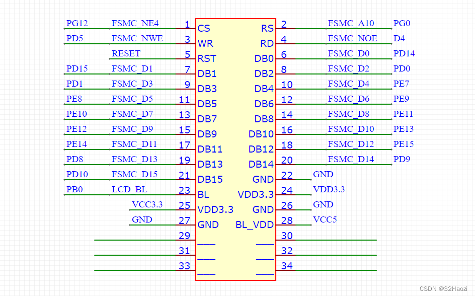
Configure FSMC
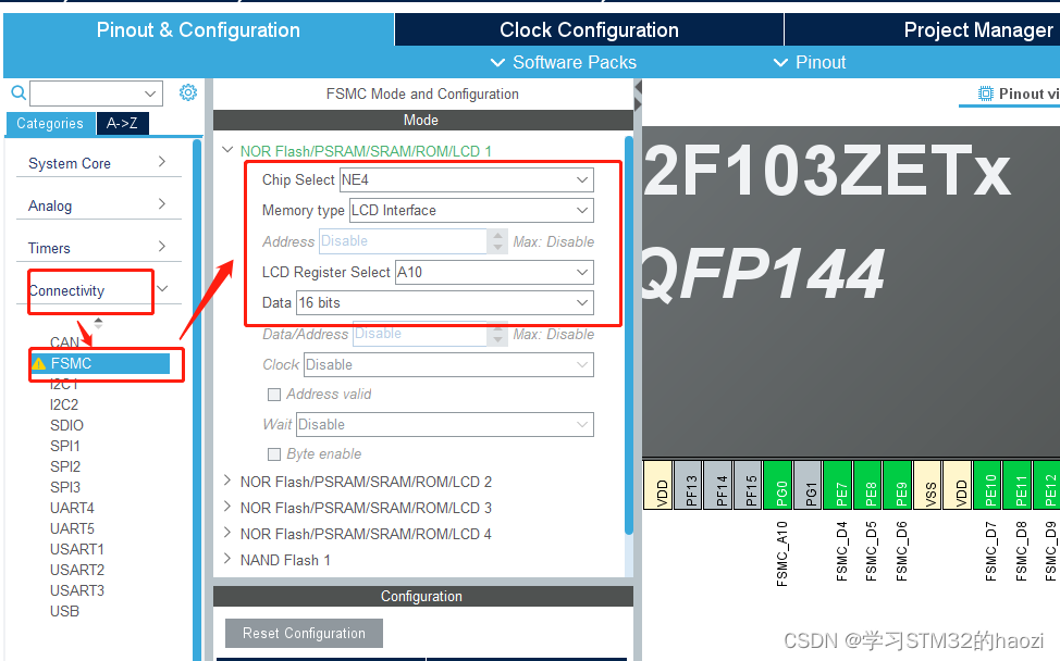
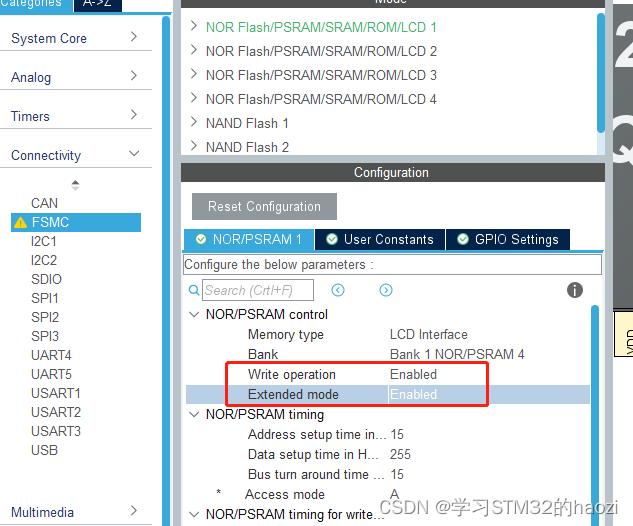
parameters to default.
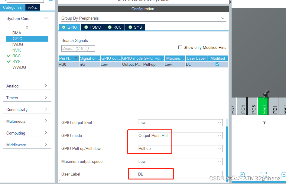
To set the backlight pin, just keep the high level directly, or configure it as PWM to adjust the brightness.
Build the project.
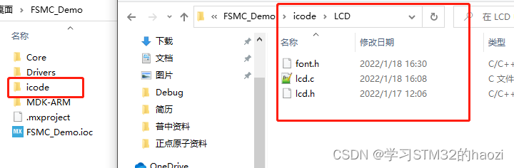
3.2. Add driver
Add icodea folder in the project directory, create a folder in the folder , and create , , and three files LCDin the folder .lcd.clcd.hfont.h
All code files are at the beginning of the article
Add source files
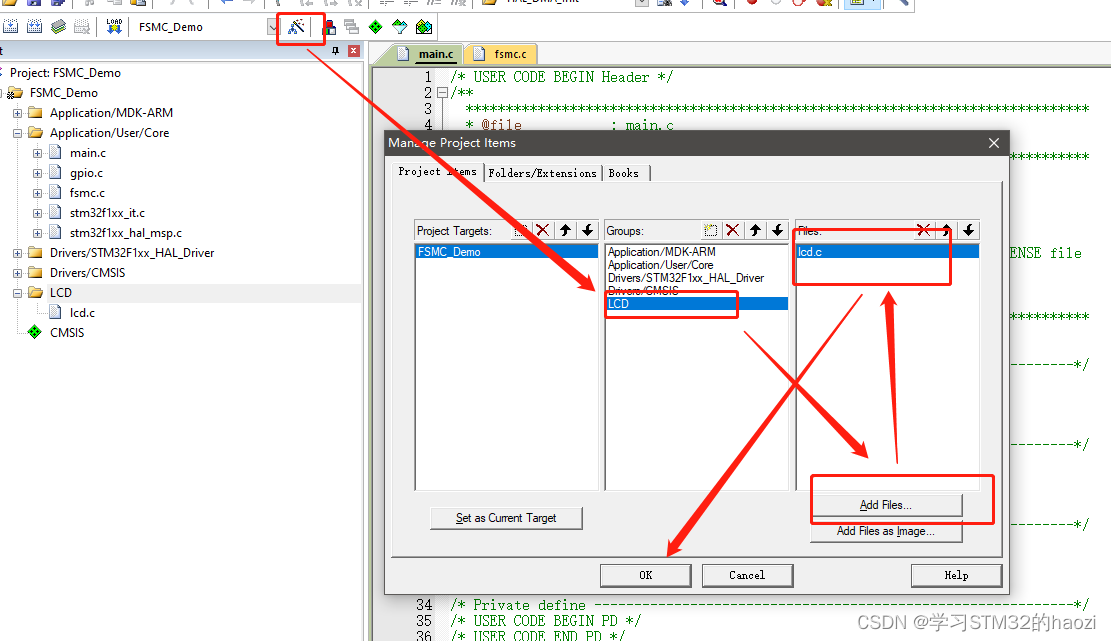
Add header file path
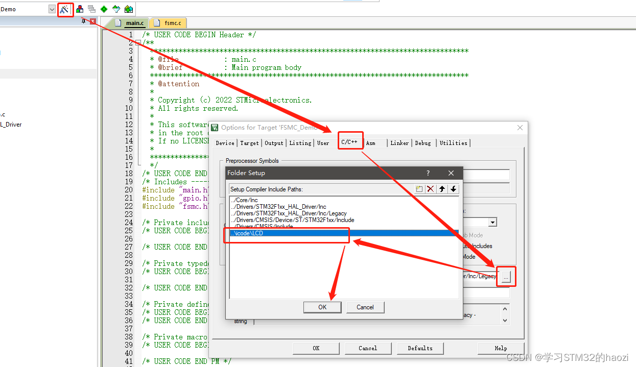
All code files are at the beginning of the article
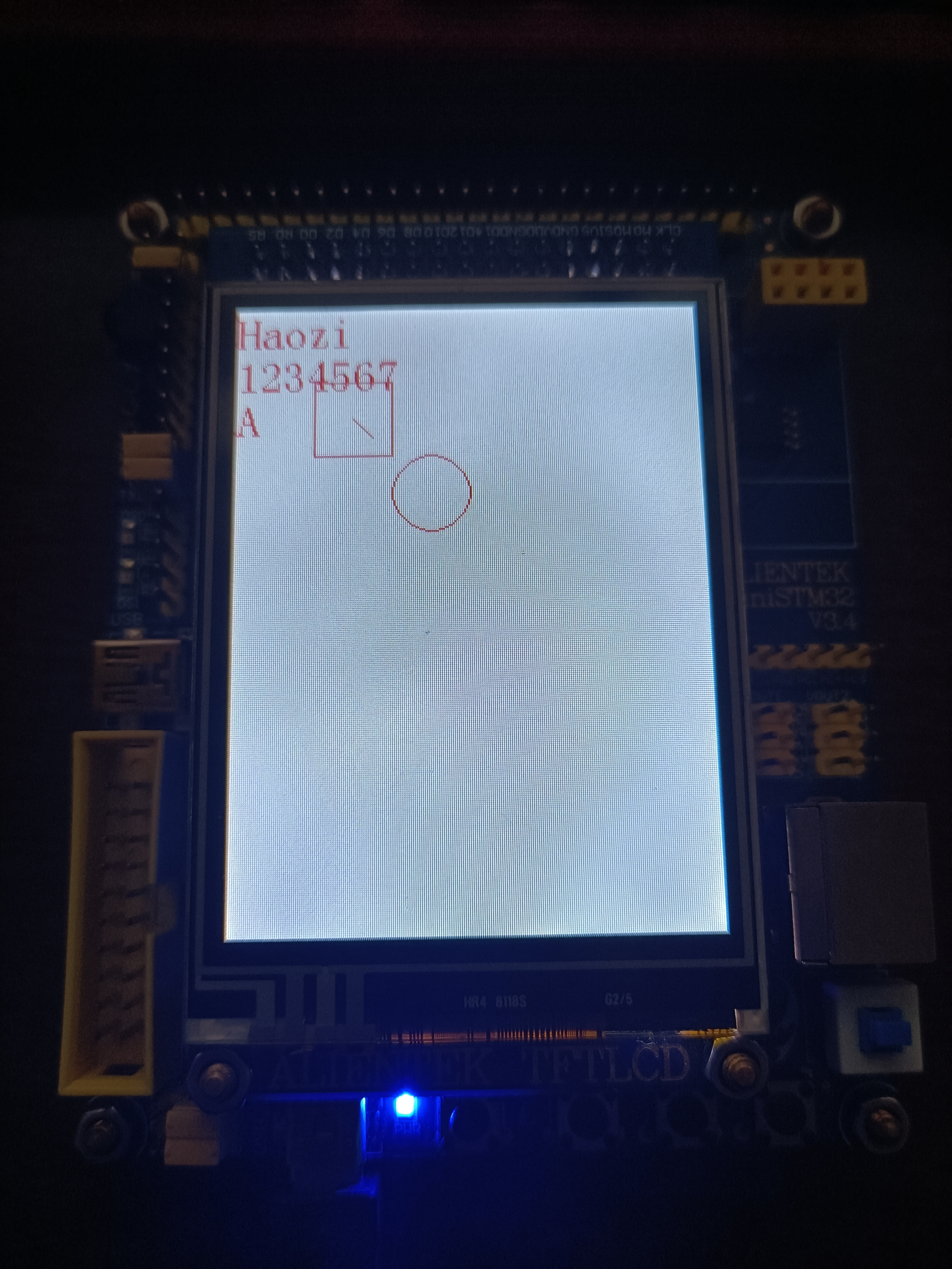
3.3. Test procedure
#include "lcd.h"

	// 其他的初始化完成之后
	LCD_Init();

	POINT_COLOR = RED;	// 画笔颜色
	LCD_ShowString(0, 0, 120, 20, 24, "Haozi");
	LCD_ShowNum(0, 24, 1234567, 7, 24);
	LCD_ShowChar(0, 48, 'A', 24, 0);

	LCD_Draw_Circle(100, 100, 20);
	LCD_DrawRectangle(80, 80, 40, 40);
	LCD_DrawLine(60, 60, 70, 70);

All code files are at the beginning of the article
4. Software simulation 8080 parallel port drive LCD
For the main controller without FSMC, it can only be driven by software simulation.
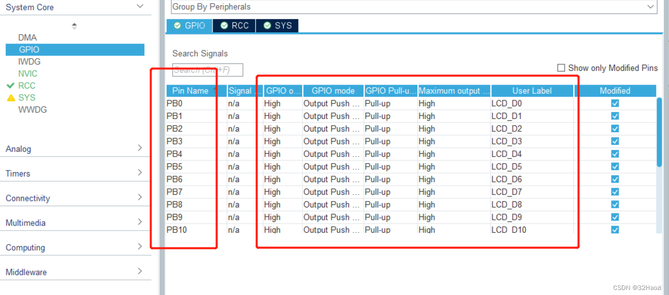
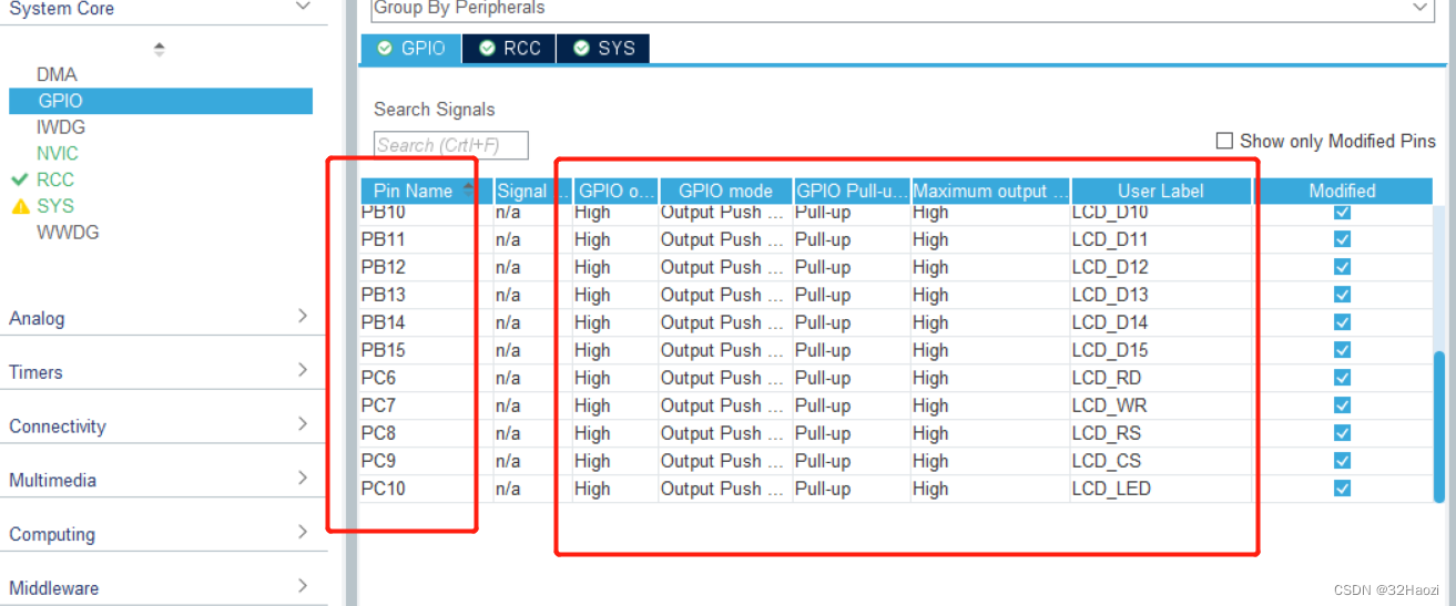
4.1. Pin configuration
Take a look at the schematic diagram of the LCD in the punctual atomic manual. In the official manual, the label in the middle of the box corresponds to the label on the ILI9341 controller.
But let's not look at this, to be consistent with the above, I will redraw the schematic diagram.
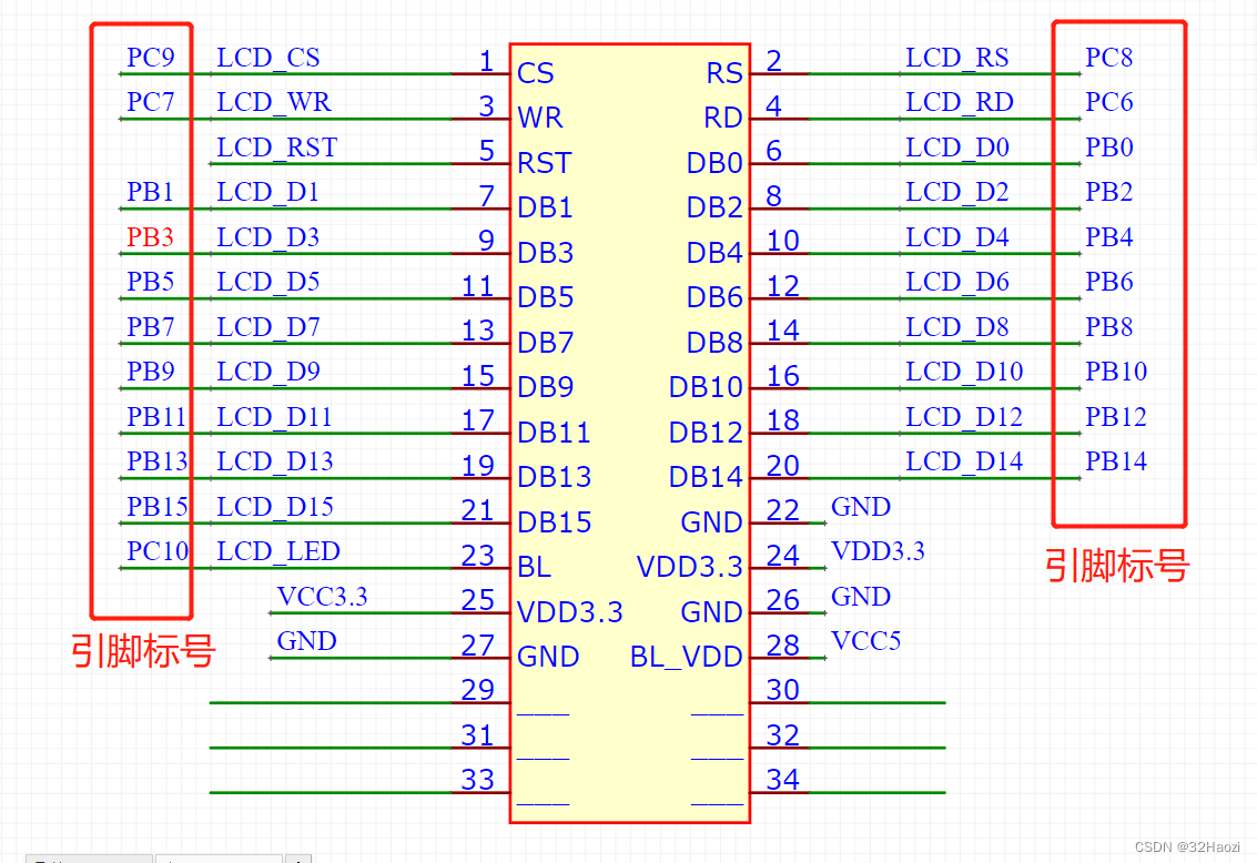
Then let's see where each pin is connected. Here we don't care about the touch function, as in the previous chapter, we only need to look at pins 1-28. The bottom six are related to the touch function, so let's ignore it.
- Pin 1 LCD_CS corresponds to PC9
- Pin 2 LCD_RS corresponds to PC8
- Pin 3 LCD_WR corresponds to PC7
- Pin 4 LCD_RD corresponds to PC6
- Pin 5 LCD_RST corresponds to the reset button of the development board
- Pins 6-21 LCD_D[17:1] correspond to PB[15:0]
- Pin 23 LCD_LED corresponds to PC10
- The rest are VCC or GND
Then configure these pins in CubeMX. PB0 - PB15, PC6 - PC10.
All are push-pull output , pull-up , output speed High .
There are 21 pins in total.
4.2. Add driver
Add icodea folder in the project directory, create a folder in the folder , and create , , and three files LCDin the folder .lcd.clcd.hfont.h
And add .c files and header files in keil.
In fact, the driver here and the driver above are basically the same in terms of external interface, but the implementation of data transmission within the function is different.
All code files are at the beginning of the article
4.3. Test procedure
The test procedure is the same as above.
#include "lcd.h"

	// 其他的初始化完成之后
	LCD_Init();

	POINT_COLOR = RED;	// 画笔颜色
	LCD_ShowString(0, 0, 120, 20, 24, "Haozi");
	LCD_ShowNum(0, 24, 1234567, 7, 24);
	LCD_ShowChar(0, 48, 'A', 24, 0);

	LCD_Draw_Circle(100, 100, 20);
	LCD_DrawRectangle(80, 80, 40, 40);
	LCD_DrawLine(60, 60, 70, 70);
All code files are at the beginning of the article
5. Supplementary Notes
After modification, only the internal implementation of the functions in lcd.c and lcd.h is different for the projects of the two driving methods. No matter which driving method you use, the interfaces called in other programs are the same.
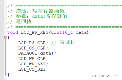
For example, in the 8080 simulation driver program, the write register function is like this.
In the code driven by FSMC, this is the case.
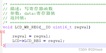
As you can see, the function names are the same and can be called in the same way. The rest of the functions are also the same.
Therefore, you don't have to think too much when transplanting, and you can use them in the same way.
Finally, this LCD screen will be used later to make a simple oscilloscope project, only a development board is needed, and this LCD screen can be realized.
The code is also open source, welcome to check it in the top article on the home page.