Interposer is an intermediate layer technology used to connect chips. Its substrate is usually a silicon substrate, and the silicon substrate is also a kind of Substrate. Therefore, Interposer has a certain relationship with Substrate. For RDL Interposer, the signal routing density of Si Interposer is further improved, which can achieve higher I/O density and lower transmission delay and power consumption. However, compared with organic substrates and RDL Interposer, the cost of Si Interposer is higher.
The following is a detailed explanation of the relevant concepts of this part
1. Substrate (substrate or substrate)
The substrate and substrate are represented by the word substrate in English. The substrate refers to the board used for electronic product packaging, which provides support and electrical connections for electronic components. The substrate material can be silicon, ceramic or organic, depending on the specific requirements of the application.
There are two most common types, one is the interconnect substrate of the silicon process, and the other is the packaging organic substrate, specifically:
(1) Interconnect substrate of silicon process
The interconnect substrate of the silicon process refers to the substrate made of silicon material, which is used for the packaging of electronic products. Silicon is a semiconductor material with high thermal and electrical conductivity, so silicon substrates are often used when packaging electronic products. The production process of silicon substrates is relatively complicated and requires multiple steps, including cutting of silicon wafers, surface treatment, substrate preparation and orientation treatment, etc. It has high thermal stability and can be used under high temperature conditions. In addition, the electrical performance of the silicon substrate is also very good, with low resistance and high capacitance, so it is very commonly used in high-frequency circuit applications. However, silicon substrates are expensive to produce because of their complex production process and expensive materials used in the production process.
(2) Encapsulation of organic substrates
Packaging organic substrate (Organic Substrate) is a substrate material commonly used in chip packaging. Its main components are organic materials, usually organic composites based on polyester, glass fiber or ceramic materials, which have low thermal conductivity and high electrical insulation properties, which make them useful in high-frequency circuit applications. Certain advantages. In addition, encapsulated organic substrates are generally less expensive to produce than silicon substrates because their production process is simpler and lower-cost materials can be used in the production process.
Although encapsulating organic substrates have some advantages, they also have some limitations. Encapsulated organic substrates have poor temperature stability and generally cannot be used at high temperatures. In addition, the electrical performance of encapsulated organic substrates is also poor, with higher resistance and lower capacitance. This limits their use in high frequency circuits (requiring more efficient transfer and storage of charge)
When selecting a package substrate, the specific requirements of the application should be considered, taking into account various factors such as material properties, production costs, temperature stability, and electrical performance.
Compared with the interconnect substrate process of the silicon process, the encapsulation organic substrate process has the huge advantages of low material and production costs and high reliability, so it is favored.
2. RDL Interposer Technology
RDL Interposer is a commonly used packaging technology, often used in the manufacture of integrated circuits and other electronic components. This technology produces a silicon substrate with through holes (TSV) on the silicon substrate by plasma etching and other technologies, and the silicon substrate can provide the interconnection basis for the chip. Fabricating redistribution layers (RDLs) on the front and back sides of the silicon substrate can provide the interconnect basis for TSVs and chips integrated on the silicon substrate. RDL Interposer technology can improve the efficiency and stability of information transmission, and has high application value in the manufacture of integrated circuits and other electronic components.
RDL (Redistribution Layer) refers to the redistribution layer, which is a technology used in electronic product packaging. It consists of metal layers and substrates, and is mainly used to connect external circuits to the internal circuits of the chip. Tiny metal pins are formed on the substrate to connect different circuits. RDL Interposer packaging technology can make the circuit connection distance between the chip and the chip smaller, make the chip packaging density higher, and greatly reduce the signal trace width and spacing, thereby increasing the signal density per unit area and improving the circuit. performance.
The main principle is to deposit metal layers and dielectric layers on the wafer surface. It forms a redistribution layer to carry the corresponding metal routing pattern and rearrange the chip's IO ports on loose areas outside the chip. Since the metal wiring formed by RDL has a smaller line width and spacing, it provides higher interconnection density, and at the same time, it can improve signal quality by shortening the circuit length, and improve chip integration capability by reducing chip area.

The traditional packaging process steps are mainly carried out after the die is cut and sliced. First, the wafer (Wafer) is cut and sliced (Dicing), and then packaged (Packaging) into various forms. Most of the process in the packaging process is to operate the wafer, that is, the overall packaging (Packaging) on the wafer, and finally the cutting and slicing.
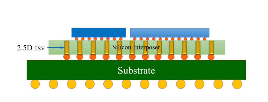
3. Silicon interposer (Si Interposer)
Interposer is an intermediary layer, often used in distributed systems, which can help exchange information between upper or lower nodes (such as connecting two chips). Interposer can usually use micro-bumps (ubump) and C4 bumps (C4 bumps) to perform electrical interconnection with chips and packaging substrates to realize information exchange between chips and packaging substrates. Interposers can be used to increase the performance and bandwidth of chips, as well as to make chips more compact.
Si Interposer technology is a traditional 2.5D packaging technology based on silicon process. This technology places an additional silicon interposer between the substrate and the die. The interconnection and communication between Dies is achieved by placing an additional silicon layer between the substrate and the die. The die is stacked on the interposer. the top of. Since the minimum pitch allowed by the bump (Bump) is not enough to support multi-chip interconnection and I/O requirements, and the silicon interposer has a high fine-pitch wiring capability, the interconnection lines are redistributed in the stacked chips.
Interconnection and communication between dies is achieved by placing additional layers of silicon between the substrate and the die, with the die stacked on top of a single interposer. Instead of using circuit boards or carrier boards as the carrier for chip connections, it can solve the packaging process bottleneck problem caused by the limit of the manufacturing process of the carrier board itself.

4. Embedded Silicon Bridge (EMIB)
Try to combine substrate technology and silicon interposer technology. It integrates small thin layers—silicon bridges—on the substrate for interconnection between chips, and embeds the silicon bridges in the packaging substrate to achieve a good balance between performance and cost.

The EMIB is a small silicon chip embedded in the underlying package substrate and provides dedicated ultra-high-density interconnects between dies. The physical size of the EMIB does not limit the number of dies that can be integrated. In contrast, alternative implementations use a large piece of Si Interposer that sits on top of the package substrate and extends over the entire length of the die to be integrated.

5. TSV (Through Silicon Vias)
Through-silicon via: A vertical interconnection structure that penetrates silicon wafers or chips, which can complete the function of connecting upper and lower wafers or chips. It is a key process for effectively improving system integration and performance in wafer multi-layer stacking. It realizes the vertical electrical connection throughout the thickness of the chip, and opens up the shortest path between the upper and lower surfaces of the chip. It is a high-density packaging technology to conduct multi-layer chip interconnection through silicon via technology. For example, memory chips and processor chips can be connected together by means of Through Silicon Vias (TSV) technology, which is no longer limited by the wiring width, line spacing, and density of the carrier board, so that the data bandwidth can be realized on the interface. improvement.

Chips are placed closer together, so there is less latency, and the reduction in interconnect length reduces associated parasitics, allowing the device to run at a higher frequency, which translates into improved performance and lower cost to a greater degree. The main advantages of TSV are as follows: