Transfer: https://blog.csdn.net/zhong_ethan/article/details/107005512?spm=1001.2014.3001.5502
Article directory
The CDC_verify_struct process mainly checks whether there are unsynchronized signals in the design and whether there are glitches. In a multi-clock design, which signals need to be considered for synchronization? What synchronization method to use? If not handled properly, metastable states or data loss can be introduced into the design . The root cause of the metastable state is insufficient setup time or hold time. This article first briefly introduces the commonly used synchronization methods of CDC, and then introduces the rules in CDC_verify_struct .
Previous: Spyglass CDC Check (3)
Next: Spyglass CDC Check (5)
synchronization method
Note: The unit of phase difference in this section is nanoseconds
Which signals need to be synchronized
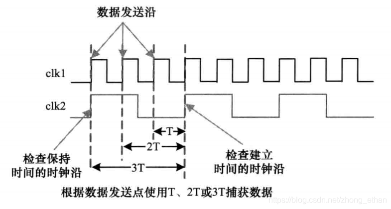
The phase difference of the effective jump edge of the clock is fixed, which is called a synchronous clock . As shown in the figure clk1 and clk2, although the frequency of the two is different, the phase difference between the active edges (rising edges) is fixed as T, 2T, 3T, so it can be called a synchronous clock.
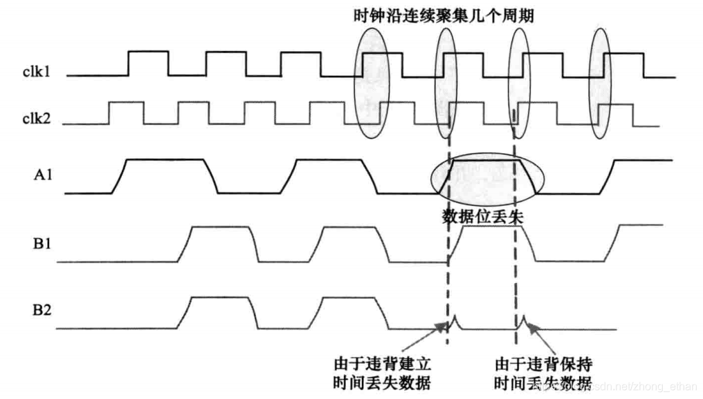
The phase difference between the effective edges of two clocks cannot be determined, which is called an asynchronous clock . The clocks of different DPLLs or crystal oscillators must be asynchronous clocks. When signals are transmitted across asynchronous clocks without synchronization, metastability and data loss can easily occur. As shown below.
Clocks from the same DPLL or crystal oscillator are called homologous clocks . Homologous clocks can be classified according to frequency and phase:
- Clock with the same frequency and zero phase difference
- Same frequency constant phase difference clock
- Non-same-frequency variable phase difference clocks, including integer multiple clocks and fractional multiple clocks.
As long as the clocks in the design are not all of the same frequency and zero phase difference, it is necessary to consider whether metastable states will be introduced during signal transmission and whether there will be data loss.
Common Synchronization Methods
Signals transferred across clock domains can be divided into two categories:
- The transmission of the control signal (usually a single bit), commonly used two-stage synchronizer.
- Transmission of data signals (usually multi-bit), common handshake signals, asynchronous FIFO method.
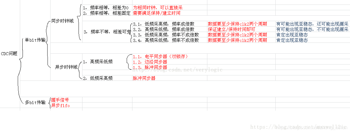
Image source: Verilog Fundamentals (Metastability and Synchronous Circuits Across Clock Domains)
Rules
AC_unsync01/02
Reports unsynchronized signals in cross-clock transfers. If this is violated, check:
- If both the source register and the destination register are in the same IP module, use ip_block to constrain this module;
- If the source register or destination register is in black_box, use abstract_port or assume_path to constrain the black_box port;
- If the source register is a static signal, use quasi_static to constrain the source register;
- If the source register is a control signal, check that the signal passes through a valid qualifier;
- If the source register is a data signal, check whether an asynchronous FIFO or handshake signal is used;
AC_sync01/02
Reports the synchronized signals in the design. This rule only reports information, not violations.
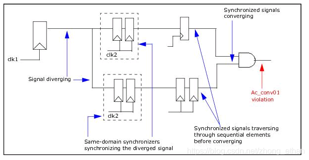
AC_conv01/02/03
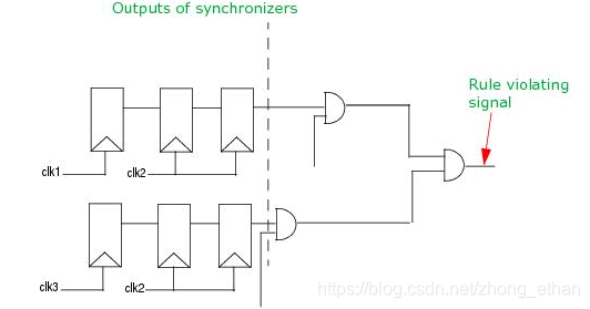
Report aggregation issues in design . Aggregation problems may cause data coherency problems, that is, the data before synchronization is inconsistent with the data after synchronization.
The AC_conv01 rule reports aggregation violations after the signal passes through the synchronizer + register:
-
After passing through the synchronizer, different signals pass through different numbers of registers, and finally aggregate at the same logic gate.
In the above example, the first signal passes through a register after passing through the second-level synchronizer, and the second signal passes through the second-level synchronizer. through two registers. These two signals end up converging at the same logic gate. Why is this a problem? Assuming that the two signals have a jump of 00->11 in the clk1 clock domain, then after passing through a bunch of registers in the clk2 clock domain, the signal will have a jump of 00->10->11 at the logic gate, obviously. It is not acceptable. If you make sure that the two signals don't jump at the same time, there is no problem, for example, the jump of 00->01 or 00->10 will not be a problem. -
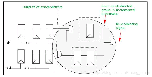
The same signal passes through multiple synchronizers and then passes through different numbers of registers, and finally aggregates at the same logic gate. This case is similar to the above case.
-
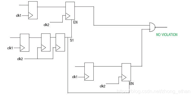
No violation will be reported in special cases : two signals are controlled by the same control signal
If spyglass reports a violation, but it is found that there is no problem with the design through inspection, you can use cdc_false_path, quasi_static, cdc_filter_conherency and other command constraints.
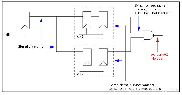
The AC_conv02 rule reports a violation of aggregation after the signal passes through the synchronizer, and passes through the register after aggregation:
- Report the problem of aggregation of different signals at the same logic gate after passing through the synchronizer.

Note that the place where the violation is reported here is different from AC_conv01. Look at the two pictures carefully. One aggregates after the register and one aggregates before the register. Why is there a problem here? Assuming that the clk1 clock and signal have 011->100 jumps, due to the different delays of each path, strange jumps such as 011->110->100 may occur after passing through the synchronizer. If this signal is a counter, then there must be a problem with this synchronization. The solution is to use Gray code encoding. Before synchronization, the binary code is converted into Gray code and then passed through the synchronizer. You can refer to Gray code pointer synchronization in asynchronous FIFO.
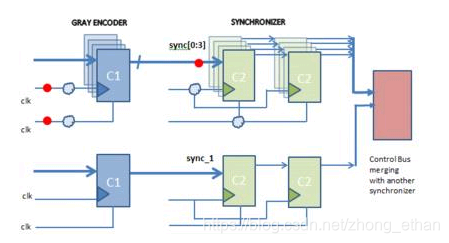
In the above example, sync[0:3] is a signal synchronized using Gray code, and sync_1 is a signal synchronized by a secondary synchronizer. They are aggregated at the same logic gate, and spyglass will report this violation. If it is determined that there is no relationship between sync_1 and sync[0:3] signals, that is, there is no problem with such a design, the following constraint script can be used
cdc_filter_coherenct -unrelated sync[0:3] sync_1
gray_signals -nam sync[0:3]
- Report the aggregation problem of the same signal at the same logic gate after passing through multiple synchronizers. The
AC_conv03 rule checks the aggregation problem of signals in different clock domains passing through the same clock domain synchronizer.
AC_glitch03
Report glitches in the design .
Competition: In a combinational logic circuit, after the same signal is transmitted through different paths, the time to reach a certain meeting point in the circuit is first and then later (the combinational logic pollution delay of each path is different), this phenomenon is called logic competition. The resulting phenomenon of output disturbance pulses is called hazard.
Risk: When the signal passes through the wiring and logic unit inside the device, there is a certain delay. The size of the delay is related to the length of the connection and the number of logic units, and is also affected by the manufacturing process, operating voltage, temperature and other conditions of the device. The high-low level transition of the signal also requires a certain transition time. Due to these two factors, when the level value of multi-channel signals changes, the output of the combinational logic has a sequence at the moment of signal change, and does not change at the same time, and some incorrect peak signals often appear. These peak signals Called a "glitch". If a "glitch" appears in a combinational logic circuit, it means that the circuit is dangerous.
Glitch: In digital circuits, a glitch is often defined as any jump that crosses the logic threshold more than once between samples. It mainly means that the output waveform of the circuit contains short, regular or irregular pulses that are useless or have other effects on the design. Deburring is generally considered.
Pulse: In electronic technology, a pulse signal is a pulse signal that is sent continuously at a certain time interval with a certain voltage amplitude. The number of pulses generated in a unit time is called the frequency. For example, when the flashlight is turned on, the light is on, which is direct current. The pulse is formed by switching the light on and off continuously, and the speed of the switch is the level of the pulse frequency.
The reason for competing adventures: The competition and adventures in digital circuits arise in combinational logic circuits. Due to the existence of delay time, when an input signal rejoins a certain gate after being transmitted through multiple paths, due to the difference in the number of stages of gates on different paths, or the difference in the delay time of the gate circuit, the time to reach the meeting point is different. Thereafter, resulting in momentary erroneous output.
The judgment for competitive adventure:As long as the logic function of the output terminal can be simplified to Y = A + A' or Y = A·A' under certain conditions, it can be judged that there is a competition-adventure phenomenon.
The resolve of competitive adventures: inserting filter capacitors, introducing strobe pulses, modifying logic design, etc.
Reprinted in: https://www.cnblogs.com/PG13/p/10329675.html
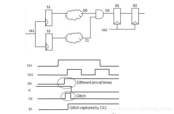
In the design shown in the figure below, D0 and I1 signals reach the AND gate at different times, and it is easy to output glitches at C0. If the glitch happens to be picked up by the register in the CLK2 clock domain, the design is prone to errors. The combinational logic of CLK1 should be modified to be a register output.
Clock_sync05/06
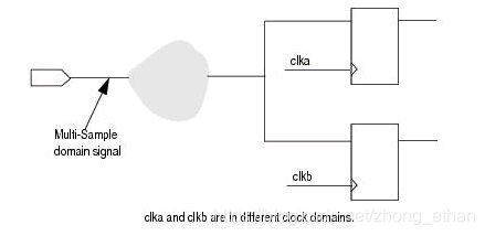
Clock_sync05 reports that the input signal is sampled by registers in multiple clock domains. As shown in the figure below, the input signal is sampled in clka and clkb.
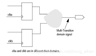
Clock_sync06 reports that the output signal is composed of multiple clock domain signals.
If there is no problem with the design, you can use the set_case_analysis or quasi_static command to strengthen the constraints on the input signal.
setup_quasi_static
Quasi-static registers mean that the input signals, registers, and nets in the design change at the beginning of chip work, but remain 0 or 1 in the next work.
 setup_quasi_static reports the quasi-static registers inferred by spyglass and the static registers constrained by the constraints script in the design . Signals should be carefully checked to see if they meet the definition of a quasi-static register. If a signal is misinferred by spyglass as a quasi-static register, then a change in that signal may cause a malfunction when the chip is operating.