BOOT pin:
Reset, start selection
The Boot pin has nothing to do with JTAG. It is only used to determine the starting address of the execution code after the MCU is started.
In the circuit design , the Boot pin may not be used, but it is required that the external resistor must be connected to ground or power supply and must not be left floating; the storage media corresponding to the three startup modes of STM32 are all built-in in the chip. They are:
User flash memory = Flash built into the chip
S RAM = RAM area built into the chip, which is memory
System memory = a specific area inside the chip. A Bootloader is preset in this area when the chip leaves the factory, which is commonly known as the ISP program. No one can modify or erase the contents of this area after the chip leaves the factory, that is, it is a ROM . district.
There are two pins BOOT0 and BOOT1 on each STM32 chip. The level status of these two pins when the chip is reset determines which area the chip starts to execute the program from after it is reset. See the table below:
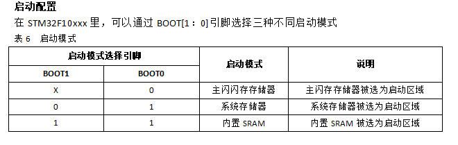
BOOT1=x BOOT0=0 Boot from user flash memory, this is the normal operating mode.
BOOT1=0 BOOT0=1 starts from the system memory. The program functions started in this mode are set by the manufacturer.
BOOT1=1 BOOT0=1 Boot from built-in SRAM, this mode can be used for debugging.
Use JTAG port or SWD mode programming to select boot from user flash memory.
When programming programs in serial port ISP mode, always choose to boot from system storage.
Programming interface
If you want to reduce the number of sockets, use SWD mode simulation . In this mode, if you use JLINK, you only need four wires. These four wires are: 3.3V, GND, SWDIO, and SWCLK.
Among them, the JTMS/SWDIO of the STM32 is connected to the TMS of the JTAG port, and the JTCK/SWCLK of the STM32 is connected to the TCK of the JTAG port. If you want to use ULINK2, add one more "N RS T", that is, 5. You can define this interface by yourself. When using it, you can use Dupont wire jumpers or make a block conversion interface board to connect the emulator and the target board.
JTAG protocol:
JTAG (Joint Test Action Group, Joint Test Action Group) is an international standard test protocol (IEEE 1149.1 compatible), also called ARM debugging protocol, mainly used for internal chip testing. Most advanced devices now support the JTAG protocol, such as ARM, DSP, FPGA devices, etc. The standard JTAG interface is 4 lines: TMS, TCK, TDI, TDO, which are mode selection, clock, data input and data output lines respectively. The relevant JTAG pins are defined as:
- TMS: Test mode selection, TMS is used to set the JTAG interface in a specific test mode;
- TCK: test clock input;
- TDI: Test data input, data is input into the JTAG interface through the TDI pin;
- TDO: Test data output, the data is output from the JTAG interface through the TDO pin;
When the JTAG protocol was defined, because computers (PCs) at that time generally had parallel ports, the parallel port was defined to be used when connecting to the computer. As for computers today, let alone laptops, there are now very few desktop computers with parallel ports. Instead, there are more and more USB interfaces. So can JTAG support the USB protocol and use the USB interface to debug ARM? This is about JLINK and ULINK.
JTAG emulator: JLink emulator, ULINK emulator, ST-LINK emulator
example:
JLINK is a JTAG-compatible emulator, used to burn in programs and debug
How does JLINK process data?
PC→USB→J-Link (via JTAG interface)→The JTAG interface circuit on STM32 directly accesses the flash through the operation register to realize reading and writing of the flash.
Note:
1. To debug ARM, you must follow ARM's debugging interface protocol, JTAG is one of them.