SEGGER J-Link Commander V7.22b(Compiled Jun 17202117:23:58)
DLL version V7.22b, compiled Jun 17202117:22:49
Connecting to J-Link via USB...O.K.
Firmware: J-Link V9 compiled May 7202116:26:12
Hardware version: V9.20
S/N:-1
VTref=3.285V
Type "connect" to establish a target connection,'?'for help
J-Link>connect
Please specify device / core.<Default>: STM32F407VG
Type '?'for selection dialog
Device>
Please specify target interface:
J)JTAG(Default)
S) SWD
T) cJTAG
TIF>
Device position in JTAG chain(IRPre,DRPre)<Default>:-1,-1=> Auto-detect
JTAGConf>
Specify target interface speed [kHz].<Default>:4000 kHz
Speed>
Device "STM32F407VG" selected.
Connecting to target via JTAG
InitTarget() start
Can not attach to CPU. Trying connect under reset.InitTarget() end
TotalIRLen =9, IRPrint =0x0011
JTAG chain detection found 2 devices:
#0 Id:0x4BA00477, IRLen:04, CoreSight JTAG-DP
#1 Id:0x06413041, IRLen:05, STM32 Boundary Scan
DPv0 detected
Scanning AP map to find all available APs
AP[1]: Stopped AP scan as end of AP map has been reached
AP[0]: AHB-AP(IDR:0x24770011)
Iterating through AP map to find AHB-AP to use
AP[0]: Core found
AP[0]: AHB-AP ROM base:0xE00FF000
CPUID register:0x410FC241. Implementer code:0x41(ARM)
Found Cortex-M4 r0p1, Little endian.
FPUnit:6code(BP) slots and 2 literal slots
CoreSight components:
ROMTbl[0] @ E00FF000
ROMTbl[0][0]: E000E000, CID: B105E00D, PID:000BB00C SCS-M7
ROMTbl[0][1]: E0001000, CID: B105E00D, PID:003BB002 DWT
ROMTbl[0][2]: E0002000, CID: B105E00D, PID:002BB003 FPB
ROMTbl[0][3]: E0000000, CID: B105E00D, PID:003BB001 ITM
ROMTbl[0][4]: E0040000, CID: B105900D, PID:000BB9A1 TPIU
ROMTbl[0][5]: E0041000, CID: B105900D, PID:000BB925 ETM
Cortex-M4 identified.
J-Link>
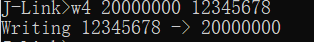
写地址 20000000 为 12345678
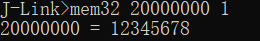
读地址 20000000 , 以验证写入正确
实验开始
第1步
J-Link>writedp 20
Writing DP register2=0x00000000(0 write repetitions needed)// 作用 : 选中 第0个AP中的第0个bank// 从0开始计数// 参数分析// writedp : 会产生 IR ,0b1010 , 选中 DPACC// 2 : 选中 Select Register // P151 In the case of a DPACC access, to read a debug port register, by the value shifted into A[3:2].// 0 : 写入 Select Register 中的值(包括选择哪个AP和选择哪个bank)
以 DDI0413C_cortexm1_r0p1_trm.pdf 分析 , 之后的 Pxx ,都是该书中的页码
分析
1. IR TDI 传入 0x1FA
P145 : On debug logic reset, IDCODE becomes the current instruction
所以,此时 必须 走 IR 链 选中 DPACC
传入 0b1010(同时TDO 0b0001) 选中 DPACC // 但是 写入的是 9bit(0x1FA),高5位无效2. DR TDI 传入 0x04
P149 : DPACC
P151 : RnW为0,表示写DATAIN[31:0]到某个寄存器 //If RnW is shifted in as 0, the request is to write the value in DATAIN[31:0] to the addressed register.
P151 : A[3:2]即TDI[2:1](值为0b10)选中寄存器P185 "AP Select Register", In the case of a DPACC access, to read a debug port register, by the value shifted into A[3:2].See JTAG-DP register map on page 9-53for the addressing details
// 注意 : DP 只有一个,AP可以有多个
P185 : AP Select Register 的 Address[3:2] 为0b10
此时标志要 写 DATAIN[31:0]即 TDI[34:3]进入 AP Select Register.// 注意 : 此次TDI传输了36bit, 高1位无效
根据 P195 "AP Select Register" 的定义 , APSEL 为0,APBANKSEL为0, 即第0个AP,第0个bank
注意 : M0 中只有一个 AP(即AHB-AP), M4 也只有一个 AP(即AHB-AP), APSEL 域 只能填入0
第2步
J-Link>writeap 120000000
Writing AP register1=0x20000000(0 write repetitions needed)// 作用 : 之前已经选中"某AP的某bank",此时写入 20000000 到该bank 中的 第1(从0开始计数)个寄存器// 参数分析// writeap : 会产生 IR ,0b1011 , 选中 APACC// 1 : 选中 Transfer Address Register // P151 In the case of a APACC access, to read an access port register, by the combination of: the value shifted into A[3:2]// 0 : 写入 Transfer Address Register 中的值(要读的地址)
以 DDI0413C_cortexm1_r0p1_trm.pdf 分析 , 之后的 Pxx ,都是该书中的页码
分析
1. IR TDI 传入 0x1FB
之前已经选中APACC,而现在要操作 APACC 组的寄存器
所以,此时 必须 走 IR 链 选中 APACC
传入 0b1011(同时TDO 0b0001) 选中 APACC // 但是 写入的是 9bit(0x1FB),高5位无效2. DR TDI 传入 0x100000002// LSB
P149 : APACC
P151 : RnW为0,表示写DATAIN[31:0]到某个寄存器 //If RnW is shifted in as 0, the request is to write the value in DATAIN[31:0] to the addressed register.
P151 :1. P151 : In the case of a APACC access, to read an access port register, by the combination of:the current value of the SELECT register in the DP, see AP Select Register,SELECT on page 9-63.
知道了当前选中的 AP 那哪个(上一条命令决定了是 AHB-AP)2. 根据 AP是哪个 A[3:2]即TDI[2:1](值为0b01) 选中寄存器P201 "Transfer Address, TAR",In the case of a APACC access, to read an access port register, by the combination of: the value shifted into A[3:2]
P201 : Transfer Address, TAR 的 offset[3:2] 为 0b01
此时标志要 写 DATAIN[31:0]即 TDI[34:3]进入 "Transfer Address, TAR"// 注意 : 此次TDI传输了36bit, 高1位无效
根据 P203 "Transfer Address, TAR" 的定义 ,Address of the current transfer 为填充为 0x20000000// 注意 (0x1 0000 0002 是 LSB)
写入后,会产生一次transter , 以 "Transfer Address, TAR" 中的值为地址, 读该地址中的内容到 该AP的 "Data Read/Write, DRW"寄存器
以 DDI0413C_cortexm1_r0p1_trm.pdf 分析 , 之后的 Pxx ,都是该书中的页码
分析
1. IR TDI 传入 0x1FB
之前已经选中APACC,而现在要操作 APACC 组的寄存器
所以,此时 必须 走 IR 链 选中 APACC
传入 0b1011(同时TDO 0b0001) 选中 APACC // 但是 写入的是 9bit(0x1FB),高5位无效2. DR TDI 传入 0x7// LSB
P149 : APACC
P151 : RnW为1,表示读某个寄存器
//If RnW is shifted in as 1, the request is to read the value of the addressed register. // The value in DATAIN[31:0] is ignored. // You must read the scan chain again to obtain the value read from the register.
P151 :1. P151 : In the case of a APACC access, to read an access port register, by the combination of:the current value of the SELECT register in the DP, see AP Select Register,SELECT on page 9-63.
知道了当前选中的 AP 那哪个(上一条命令决定了是 AHB-AP)2. 根据 AP是哪个 A[3:2]即TDI[2:1](值为0b11) 选中寄存器P201 "Data Read/Write, DRW",In the case of a APACC access, to read an access port register, by the combination of: the value shifted into A[3:2]
P201 : Data Read/Write, DRW 的 offset[3:2] 为 0b11
此时标志要 读 P204 "Data Read/Write, DRW"
注意 : 之前讲述的
1. The value in DATAIN[31:0] is ignored.2. You must read the scan chain again to obtain the value read from the register.
TODO : 要读哪个寄存器? 猜测是 DPACC 中的 "Read Buffer"3. DR TDI 传入 0x1FA// LSB
选中 DPACC
4. DR TDI 传入 0x7, TDO 传出 0x91A2B3C2// 实际传送了 36bit , 最高为无效
RnW 为1,表示读
TDI[2:1] 为 0b11 , 对应 P185 中的 "Read Buffer"
TDI[34:3] 被忽略
TDO的[34:3] 是 value
TDO[3] 是 第1个字节的最低位
0x91A2B3C2:000010010001101000101011001111000010:{
0}0001001000110100010101100111100[0]010// [0] 为 TDO[3] , {0} 为无效位:12345678