1, Camera imaging principle introduction
Camera work flow chart
Camera imaging principle can be summarized as follows:
Scene ( the SCENE ) through the lens ( the LENS generated) an optical image projected onto the image sensor (the Sensor) on the surface, and then converted to an electric signal , after A / D (analog-digital conversion) after conversion becomes the digital image signal , and then sent to a digital signal processing chip (DSP) are processed -> RGB image data, then through the IO interface to the transmission CPU processing by DISPLAY can see the image.
A charge coupled device (CCD) or a complementary metal oxide semiconductor (CMOS) receives the optical lens to the image passed through the analog / digital converter (A / D) converted into a digital signal, after the code storage.
Process is as follows:
. 1, the CCD / object to the CMOS optical signals into electrical signals - an electronic image (analog signal)
2, by an analog / digital converter (ADC) chip to the analog signal into a digital signal
3, the digital signal after formation, the signal is compressed or coded by the DSP library and converted to a specified format image file storage
Digital camera optical lens with the same conventional cameras, the image sensing device to the polyethylene, i.e., (light) charge coupled device (the CCD) . CCD cameras replacing the traditional photographic film position, which is a function of the optical signal is converted into an electrical signal , the same as the TV camera.
A CCD is a semiconductor device , the core of a digital camera, which is the number of cells contained in the device determines the digital camera image quality - the pixel , the more cells , i.e. a high number of pixels , image quality is better , usually low pixel representatives a digital camera quality and technical specifications .
2, Android Camera frame
Android's Camera subsystem provides a framework for taking pictures and recording video.
It will apply to the upper Camera Application Framework, the user library connected in series, and it is the user library to communicate Camera hardware layer and to achieve operating camera hardware.
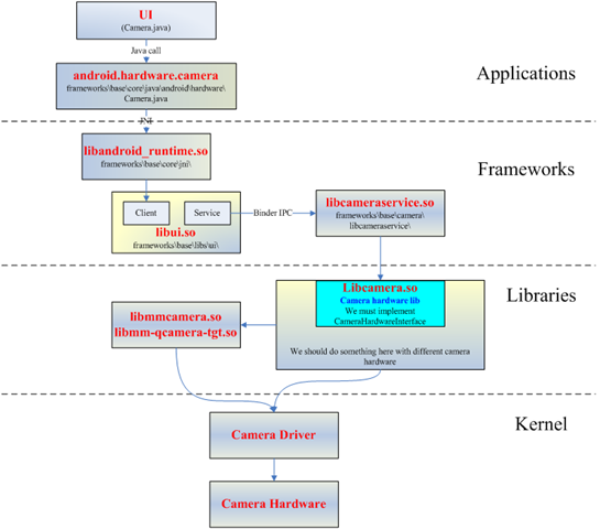
3, Android Camera code structure
Camera's Android code is mainly in the following directories:
Camera portion of JAVA
packages / apps / Camera /. Camera.java file which is the main achievement. This section is compiled into goal Camera.apk
com.android.camera this package, several major class file as follows:
PhotoViewer: GalleryPicker.java (all images set) ---> ImageGallery.java (under a picture Folder List ) ---> ViewImage.java (see photos of a specific picture)
the VideoPlayer: GalleryPicker.java (all video set) ---> MovieView.java (watch a video)
Camera: Camera.java (Camera viewfinder and camera)
videocamera : VideoCamera.java (videoCamera viewfinder and camera)
The framework for the upper part of the Camera application calls
base/core/java/android/hardware/Camera.java
This part of the goal is framework.jar
Camera JNI part of
frameworks / base / core / jni / android_hardware_Camera.cpp
This section is compiled into goal libandroid_runtime.so.
Camera UI library section
frameworks / base / libs / ui / camera
content of this section is compiled into a library libcamera_client.so.
Camera Services section
frameworks / base / camera / libcameraservice /
This section is compiled into a library libcameraservice.so.
Camera HAL layer portion
hardware / msm7k / libcamera
or
vendor / qcom / android-open / libcamera2
order to achieve a particular function Camera, the HAL layer requires a hardware-related Camera library (e.g., by calling video for linux drivers and Jpeg encoding program implement or to direct a private library with various chip manufacturers to achieve, such as Qualcomm achieved libcamera.so and libqcamera.so), implements the interface prescribed CameraHardwareInterface, to call the relevant library, drive-related driver, realize the operation of camera hardware . This library is the library libcameraservice.so Camera service calls.
To be continued
In the next article, I will detail two paths to achieve Camera HAL: The basis V4l2 own specifications to achieve CameraHardwareInterface; Qualcomm's Camera architecture (QualcommCameraHardware and mm-camera / mm-still). Of course, when it comes to Qualcomm private library section, in order to avoid unnecessary trouble, I will be passing. Please forgive me!
Qualcomm Android platform hardware debugging of the Camera
Debugging on android platform Qualcomm paragraph 2 camera sensor, is an OV of 5M YUV sensor, supports jpeg out, also supports AF, debugging relatively simple, because other projects already in use, just put on transplant-related drive good; the other is Samsung's a relatively new 3M YUV FF sensor, the latest project to be used in this paper to debug the sensor, for example, to share the experience from the perspective of the underlying driver debugging camera at Qualcomm android platform, As for the Qualcomm platform architecture and the principle part of the camera is not too much introduction.
First, the preparatory work
from the project seen before hardware (board) ready, the software part is to be prepared. Separately from the bottom view of the drive, the software portion can be divided into two parts, a high-pass platform dependent, then one is common practice to sensor portion of the sensor related is transplanted into the frame is set to a high-pass platform. So we need to get the sensor register setting file sensor's spec and vendors. Spec purpose is apparent and a high-pass sensor communications platform (write register) and the related timing parameter setting; the setting file provided by the manufacturer is using various camera functions (preview, snapshot ...) when the sensor needs to be written middle.
In this project, Qualcomm platform MSM7X27, camera is Samsung 5CA. Is known from the spec, the sensor's I2C ID is 0x78, I2C communication using the double-byte mode, additional rules are also clear the register read sensor, from the standpoint debugging substantially enough. Also setting file provided by the manufacturer, in fact, the register list, then tell us what time to write what values which registers, usually a register address plus the value of the register, but the text is provided by Samsung PC debugging use, You need to convert itself into a two-dimensional array c language. Seen from the file, the data register can be divided into several parts: initialization, setting the IQ (Tuning related), CLK is set, preview setting, Snapshot set, there are several substantially enough, such as the regulation of other brightness matter, it set a special effect, it is provided a white balance, etc., can be accomplished by their spec.
Sensor rear portion get something, the next step is to modify the drive portion of the high-pass camera, there are:
Kernal parts:
1. Sensor Check power configuration, and modify the settings in the software. This project using 2.8 / 1.8 / 1.5 power of 3.
2, sensor reset check and modify settings. Note that reset time setting, be sure to spec and consistent, otherwise it will lead sensor does not work.
3, modified I2C driver, double byte read interface, and completion of reading sensor ID of the interface. This is used to verify whether the I2C communication the OK
. 4, introduced into register set, the corresponding register values are written in several parts of initialization, preview, snapshot and the like.
Note: reset and write registers section must add some delay in accordance with the provisions of the spec, otherwise it will lead to abnormal sensor work
User space segment:
This part is to configure the hardware specifications of VFE, such as format, interface mode, resolution, size, pattern sync signal sensor output data, etc., is relatively simple, but be sure to double-check, will not lead anywhere debugging failures.
Up to this point, the software part of the preparation has come to an end.
Second, the debugging environment to prepare (the board came out, but not in place sensor sample)
First, the test point preparation.
Before commissioning will need to think well, if the sensor does not work, how to debug, which requires to measure some signals, such as power, reset, I2C, M / P CLK, H / V sync signals, data signals, etc., to ensure that these signal can be measured.
Second, we must choose the software debugging environment, here choose to perform Qualcomm mm-qcamera-test program in the ADB to debug environment, the relevant trace can be printed out.
So everything is ready, only the sensor.
Third, debugging (sensor finally got)
a sensor connected to the board, boot, ADB run the debugger, preview the picture did not come out, fail, a little disappointed, thought that possible in one go, but after all this is a new sensor, anywhere do not think the bit position will lead to failure. Then find the reasons for it.
1, the trace that first, the sensor read has I2C ID: 0x05CA, which may account I2C communication is no problem
2, then check the Sensor power configuration, the measured power supply sensor 3, is the OK.
3, measuring the MCLK, is provided to the sensor used, normal (24MHZ)
. 4, measuring the PCLK, the sensor output is normal (58MHZ, the upper limit of the high-pass 96MHz), and the same configuration registers.
5, measurement H / V sync signal, the output of the sensor is normal. And FPS and resolution unanimously.
6, the measurement data signal, the output of the sensor is normal. (Data signal can be seen on the oscilloscope)
It would appear, sensor has to work in, but why the preview screen does not come out of it? Qualcomm continues to check the side of the set.
From the trace of view, Qualcomm VFE has been reset and start, but a direct no output preview data, which is strange, sensor clearly has an output, why after VFE received and no data spit it, do data the sensor output VFE is not recognized? To verify this, I measured on the other board OV sensor output waveform data, mainly M / P clk, H / V sync signal, and then used to compare, but did not unusual, but the H / V sync signals differ, the main level of the duty cycle is not consistent, so that the signal will not be the problem it? To further validate, I measured simultaneously H / V signal and a data signal, the data signal then found OV sensor output is in the low level V packet frame synchronization signal; and a data signal is outputted from Samsung 5CA frame packet V high-level sync signals, will not be because V signal polarity setting does not lead to VFE sensor output data read into it? Re-checked the Qualcomm VFE set, and she has a V parameter is used to set the polarity of the signal, this parameter defaults to Active Low, I am here not to modify it. Then use this parameter to Active High, re-build, after the download, the boot operation, Ok a, preview screen display properly. Up to this point sensor hardware debugging can be counted as complete, follow other functions can also be gradually improved.
FSL debugging purposes Camera
fsl the camera hal upper layer does not implement the interface setting parameters to the lower layer, it needs its own implementation. Fortunately, from the application layer to the parameter hal already running again, otherwise the workload is even greater.
Hal layer parameter setting function call is status_t CameraHal :: setParameters (const CameraParameters & params). Implement settings for each parameter in this function inside. Parameter setting CameraParameters achieved mainly through the class. This class is found by observation, which has a get () function, the parameters can be obtained, respectively. The
const char * white_balance = params.get (CameraParameters :: KEY_WHITE_BALANCE); this parameter can be obtained, i.e., the return value of the current white balance. The return value is then determined which is the case, such as
if (strcmp (white_balance, CameraParameters :: WHITE_BALANCE_AUTO) == 0) {// is determined that the automatic white balance
logV ( "Auto white_balance to the ioctl IS / n-!");
CTL. id = V4L2_CID_AUTO_WHITE_BALANCE; // automatic white balance command, ctl as v4l2_control structure which is useful
ctl.value =. 1;
IF (the ioctl (camera_device, VIDIOC_S_CTRL, & ctl) <0) {// by VIDIOC_S_CTRL pass down the structure ctl
the LOGE ( "SET Control failed / n-");
// return -1;
}
} else if (strcmp (white_balance, CameraParameters :: WHITE_BALANCE_INCANDESCENT) == 0) {// incandescent mode
logV ( "IS Incandescent white_balance to the ioctl / n-!");
ctl.id = V4L2_CID_DO_WHITE_BALANCE; // balance other cases this command
ctl.value = 2; // white balance mode according to user-defined number of permutations
if the same structure by VIDIOC_S_CTRL pass on the ctl (ioctl (camera_device, VIDIOC_S_CTRL, & ctl) <0) {//, then in accordance with value the value of points of the discussion
the LOGE ( "SET Control failed / n-");
// return -1;
}
}
mxc_v4l_ioctl transmitted to the driving of mxc_v4l2_capture.c file, mxc_v4l_ioctl call mxc_v4l_do_ioctl, mxc_v4l_do_ioctl following explanation of the command
/ *!
* VIDIOC_S_CTRL the ioctl V4L2
* /
Case VIDIOC_S_CTRL: {
pr_debug ( "Case VIDIOC_S_CTRL / n-");
retval = mxc_v4l2_s_ctrl (CAM, Arg);
BREAK;
}
This to mxc_v4l2_s_ctrl. In the case of sub-mxc_v4l2_s_ctrl by calling ctl.id
Switch (the C-> ID) {
......
Case V4L2_CID_AUTO_WHITE_BALANCE:
ipu_csi_enable_mclk_if (CSI_MCLK_I2C, CAM-> CSI, to true, to true);
RET = vidioc_int_s_ctrl (CAM-> Sensor, c); // this function is driven in v4l2 correspond ov7670 s_ctl
ipu_csi_enable_mclk_if (CSI_MCLK_I2C, CAM-> CSI, to false, to false);
BREAK;
Case V4L2_CID_DO_WHITE_BALANCE:
ipu_csi_enable_mclk_if (CSI_MCLK_I2C, CAM-> CSI, to true, to true);
RET = vidioc_int_s_ctrl (CAM-> Sensor, C);
ipu_csi_enable_mclk_if (CSI_MCLK_I2C, CAM-> CSI, to false, to false);
BREAK;
......
wherein vidioc_int_s_ctrl () is driven in v4l2 correspond ov7670 ioctl_s_ctrl, since the specific code corresponding to how space reasons not posted.
The id Points to achieve ctl structure can.
switch (vc-> id) {
.....
case V4L2_CID_AUTO_WHITE_BALANCE:
retval = ov7670_autowhitebalance(vc->value);
break;
case V4L2_CID_DO_WHITE_BALANCE:
retval = ov7670_dowhitebalance(vc->value);
break;
......
下面是whitebalance函数的实现
static int ov7670_autowhitebalance(int value)
{
unsigned char v = 0;
int ret;
printk("0v7670_autowhitebalance called/n");
ret = ov7670_read(ov7670_data.i2c_client, REG_COM8, &v);
if (value)
v |= COM8_AWB; //自动白平衡
msleep(10); /* FIXME */
ret += ov7670_write(ov7670_data.i2c_client, 0x01, 0x56);
ret += ov7670_write(ov7670_data.i2c_client, 0x02, 0x44);
ret += ov7670_write(ov7670_data.i2c_client, REG_COM8, v);
return ret;
}
static int ov7670_dowhitebalance(int value)
{
unsigned char v = 0;
int ret;
printk("0v7670_dowhitebalance called value:%d/n",value);
ret = ov7670_read(ov7670_data.i2c_client, REG_COM8, &v);
if (value)
v &= ~COM8_AWB; //关闭自动白平衡
msleep(10); /* FIXME */
ret += ov7670_write(ov7670_data.i2c_client, REG_COM8, v);
if(value == 2) //INCANDESCENCE //这个值就是ctl的value值
{
ret += ov7670_write(ov7670_data.i2c_client, 0x01, 0x8c);
ret += ov7670_write(ov7670_data.i2c_client, 0x02, 0x59);
}else if(value == 3) //FLUORESCENT
{
+ = ov7670_write RET (ov7670_data.i2c_client, 0x01, 0x7E);
RET = + ov7670_write (ov7670_data.i2c_client, 0x02, 0x49);
} the else IF (value ==. 4) the DAYLIGHT //
{
RET = + ov7670_write (ov7670_data.i2c_client, 0x01, 0x52);
RET = + ov7670_write (ov7670_data.i2c_client, 0x02, 0x66);
}
return RET;
}
wherein the function ox01,0x02 are blue and red channel gain register.
Hal layer from above the final white balance sensor to the process parameters. Other effects such as color, are the same view mode process.
Particular view mode setting register depending on the circumstances, such as night mode to
the color effect is mainly achieved by setting the value of the uv
