W25Q64 serial FLASH basics
Size : 8M (Byte) (128 block (Block), 64K bytes per block, each block of 16 sectors (Sector), 4K bytes per sector, each sector 16 of 256 bytes )
features : Flash chip within the data only by 1 to 0, from 0 to 1 can not be changed.
W25Q64Flash work :
. 1) W25Q64 SPI data transfer timing W25Q64 support SPI data transmission timing mode 0 (CPOL = 0, CPHA = 0) and mode 3 (CPOL = 1, CPHA = 1), Mode 0 and Mode 3 The main difference is that when SPI hardware interface when the host is in an idle state, level state SCLK is high or low. For Mode 0 is, SCLK is at a low level; for Mode 3 is, SCLK is high. However, in both modes, the input chips are collected at the rising edge of SCLK, the falling edge of the output data.
2) W25Q64 W25Q64 data format data format is a data size of length 8, starting high, low recurrence. 3) W25Q64 W25Q64 support transmission speeds in standard mode 80M bit / s rate, support 160M bit / s speed fast mode, supports 320M bit / s high speed mode speed.
View Serial FLASH chip
CE: CE is a chip select pin, active low. After power until a new instruction is executed, you must make / CE pin to have a falling edge.
SO (MISO): SO is the serial data output pin, the output data on the falling CLK (serial clock) pin. WP: WP write protect pin for the active level is low. Readable and writable high-level, low-level read only. SI (MOSI): SI is the serial data input pin, data, address and command from the input SI to the chip pin, data captured in the capture rising CLK (serial clock) pin.
CLK (SLCK): CLK pin is the serial clock. SPI clock pin, the clock pulse input to output. HOLD: HOLD pin is held active low. When CE is low, and the HOLD low, the data output pin is high impedance, and will ignore the signal on the data input pin and a clock pin. The HOLD pin is pulled, the device resumes normal operation.
VCC: The supply 2.7V ~ 3.6V.
GND: ground
W25Q64 principle of operation
SPI interface, by sending a corresponding command to flash the standard SPI protocol, and then flash various related operations according to the command.
① Write Enable: 06H
② read status register instruction: 05H
③ Write Status Register instruction: 01H
④ read data: 03H ⑤ Page Write: 02H
⑥ Sector Erase command: 20H
⑦ block erase command: D8H
⑧ chip erase command : 07H
⑨ down command: B9H
⑩ read ID command: 90H
QSPI Basics
QSPI is short for Quad SPI, SPI is a Motorola company launched expansion interface, and more extensive than SPI applications. On the basis of the SPI protocol away, Motorola its function has been enhanced, increasing the transport mechanism queue, the queue introduced Serial Peripheral Interface protocol (i.e., protocol QSPI). QSPI is a dedicated communication interface, connected to single, double or quad (data lines) SPI Flash storage medium.
The interface can work in three modes:
Indirect mode : all of the operations performed using the QSPI register
status polling mode : Flash status register read cyclically outside, and generates an interrupt flag (e.g., erase or programming is done 1 An interrupt is generated)
memory mapped modes : external Flash mapped to the address space of the microcontroller, so that the system be regarded as the internal flash memory dual mode, access two Quad-SPI Flash, can improve the throughput and capacity twice.
QSPI Features
• QSPI can be connected using six signals Flash, are four data lines BK1_IO0 ~ BK1_IO3, an output clock CLK, a chip select output (active low) BK1_nCS,
their effects are described below:
• BK1_nCS: chip select output ( active low) for FLASH 1. If QSPI flash always operating in dual mode, it can also be used FLASH 2 device select signal line. QSPI communication line is set to the low level BK1_nCS start signal to BK1_nCS line high as the end signal.
• CLK: clock output for two memory for synchronizing data communication. It is generated by the communications host, determines the rate of communication, different devices support the highest clock frequency is not the same as the clock frequency of the STM32 QSPI maximum fpclk / 2, when the communication between the two devices, the communication rate is limited to a low-speed device .
• BK1_IO0: in two-wire / four-wire mode bidirectional IO, single-line mode for serial output suitable for FLASH 1.
• BK1_IO1: in two-wire / four-wire mode bidirectional IO, single-line mode for serial input applied to FLASH 1.
• BK1_IO2: In four-wire mode is a bidirectional IO, suitable for FLASH 1.
• BK1_IO3: In four-wire mode is a bidirectional IO, suitable for FLASH 1.
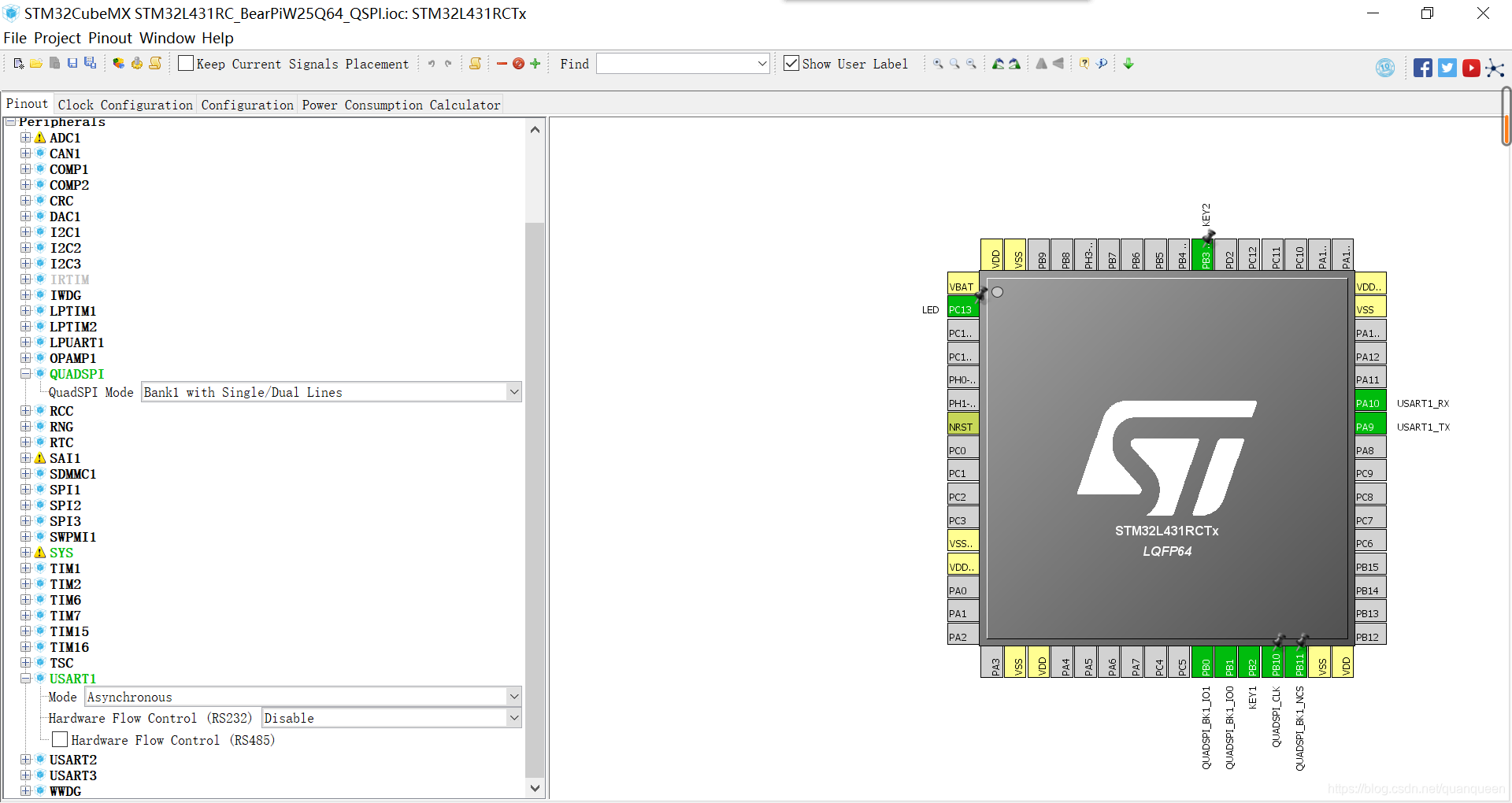
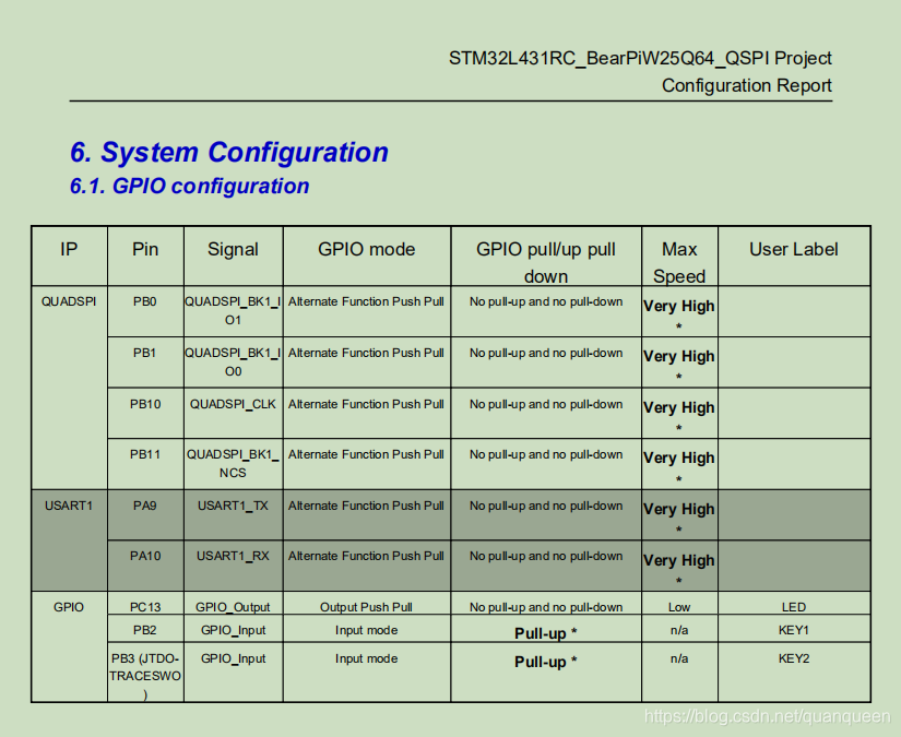
View pins
① QUADSPI_BK1_IO1 of pins PB0
② QUADSPI_BK1_IO0 as PB1 pin
③ QUADSPI_CLK as PB10 pin
as QUADSPI_BK1_NCS PB11 pin ④
⑤ to the LED pin PC13
transmission PA9 pin ⑥ is UART1
UART1 receive the pin ⑦ of PA10
as PB2 primer ⑧ key KEY1 foot
⑨ key KEY2 to PB3 pin
Pin Configuration
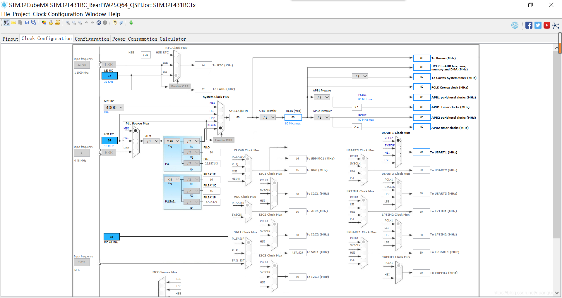
Configuring the Clock
Using the internal clock (default) the system clock up to 80MHZ
Configuration QSPI
Prescale factor //
// threshold value in the FIFO
// sample shift
// size of the Flash
// chip select high time
// Clock Mode

QSPI generation project
1, custom project name.
2. Select English path, otherwise it will lose boot files can not be compiled by the need to manually add the startup file: startup_stm32l431xx.s
3, select MDK-ARM V5 development software, namely KEIL5 software.
Code written instructions
1、移植QSPI驱动。
2、按键KEY1按下时,擦除一个扇区,并在一个位置写入数据1。
3、按键KEY2按下时,擦除相同扇区,并在另一个位置写入数据2。
4、按复位键,查看两个位置写入的数据。
调用函数:
1、QSPI_CommandTypeDef;
2、HAL_QSPI_Transmit(QSPI_HandleTypeDef *hqspi, uint8_t *pData, uint32_t Timeout);
3、HAL_QSPI_Receive(QSPI_HandleTypeDef *hqspi, uint8_t *pData, uint32_t Timeout);
4、HAL_QSPI_Command(QSPI_HandleTypeDef hqspi, QSPI_CommandTypeDef cmd, uint32_t Timeout);
5、调用QSPI驱动的读取芯片ID函数,擦除写入函数,读取数据函数。
6、HAL_GPIO_ReadPin(GPIO_TypeDef GPIOx, uint16_t GPIO_Pin);//检测按键 7、void HAL_Delay(uint32_t Delay);//延时
8、HAL_GPIO_TogglePin(GPIO_TypeDef GPIOx, uint16_t GPIO_Pin);//点亮和熄灭LED
9, printf (); // print data to the serial port functions need to be re-defined functions fputc (); you can use normal printf ();
rewrite fputc () enables the printing data to the serial port
int fputc(int ch,FILE*f)
{
	uint8_t temp[1]={ch};
	HAL_UART_Transmit(&huart1,temp,1,2);
	return HAL_OK;
}
Coding to achieve
Define the variable:
 uint32_t location1=0;
 uint32_t location2=100;
 uint32_t W25xID; uint16_t ReadData[]={0};
 uint16_t ReadData_1[]={0};
 uint8_t writeData[]={"welcome to IoT"};
 uint8_t writeData_1[]={"第一个QuadSPI实验"};
while (1) an outer loop
hal_spi_flash_read(ReadData,sizeof(writeData),0);//读0位的数据 printf("ReadFlashData:%s\r\n",(char*)ReadData);//打印读出的数据 hal_spi_flash_read(ReadData_1,sizeof(writeData_1),100);;//读100位的数据 printf("ReadFlashData_1:%s\r\n",(char*)ReadData_1);//打印读出的数据 W25xID=hal_spi_flash_get_id();//读取芯片ID
Coding to achieve
while(1)循环内 代码编写实现 if(HAL_GPIO_ReadPin(KEY1_GPIO_Port,KEY1_Pin)==GPIO_PIN_RESET)
{
		HAL_Delay(100);
		if(HAL_GPIO_ReadPin(KEY1_GPIO_Port,KEY1_Pin)==GPIO_PIN_RESET)
	 	{
	  			printf("KEY1 Press \r\n");
	  			printf("W25xID:%x\r\n",W25xID); /*最小擦除为4096,所以一次就要擦除0-4096位置,然后在0-4096的任意位置写入数据*/
	  			hal_spi_flash_erase_write(writeData, sizeof(writeData),0);
	  	}
}
if(HAL_GPIO_ReadPin(KEY2_GPIO_Port,KEY2_Pin)==GPIO_PIN_RESET)
{
		HAL_Delay(100);
		if(HAL_GPIO_ReadPin(KEY2_GPIO_Port,KEY2_Pin)==GPIO_PIN_RESET)
		{
				printf("KEY2 Press \r\n"); printf("W25xID:%x\r\n",W25xID); /*最小擦除为4096,所以一次就要擦除0-4096位置,然后在0-4096的任意位置写入数据*/
				hal_spi_flash_erase_write(writeData_1, sizeof(writeData_1),location2);
		 }
}
