Article directory
- 1. General register of 8086
- 2. 8086 memory access and byte order
- 3. Program segmentation
- 4. Program relocation problems
- 5. Segment address and offset address
- 6. 8086 memory access dilemma
- 7. 8086 strategy for selecting segment addresses
- 8. Memory access process of 8086
- 9. Flexibility of logical addresses and segmentation
1. General register of 8086
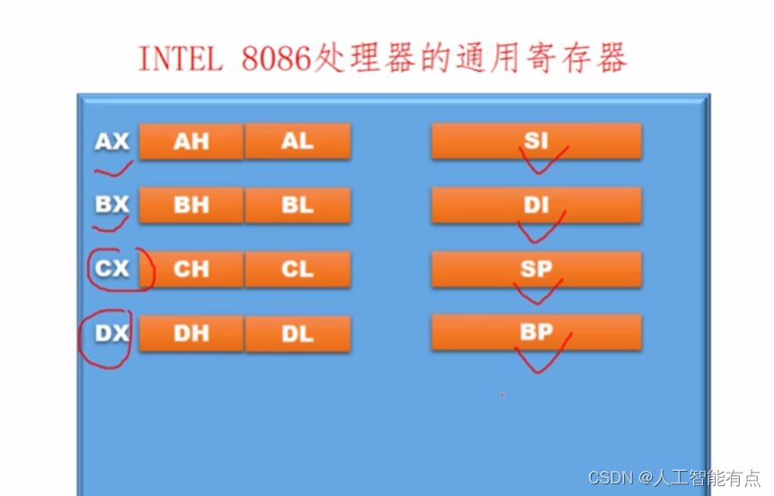
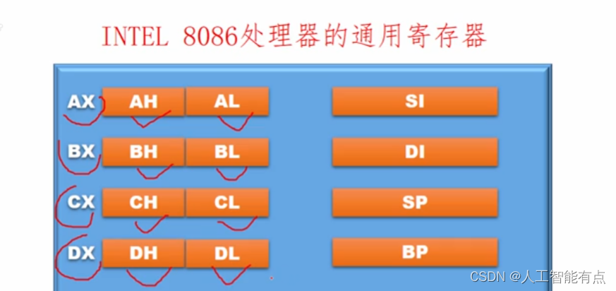
The 8086 processor has eight 16-bit general-purpose registers.
What is the lowest bit in the register? What is the highest position? How to differentiate?
Answer: The high position is on the left and the low position is on the right. As shown in the figure:
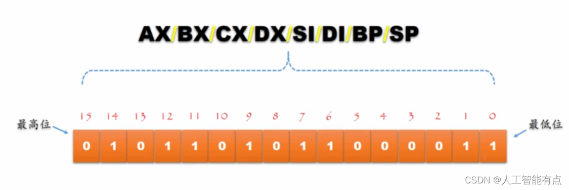
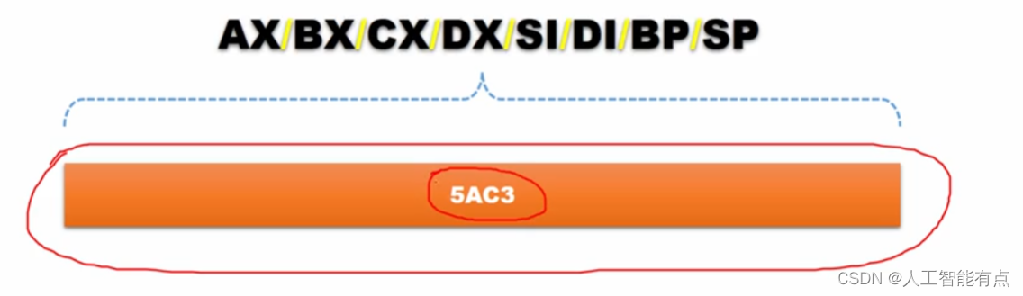
the highest bit of the data stored in this 16-bit register is 0 and the lowest bit is 1. However, for convenience, the register contents are generally given in hexadecimal. As shown below:
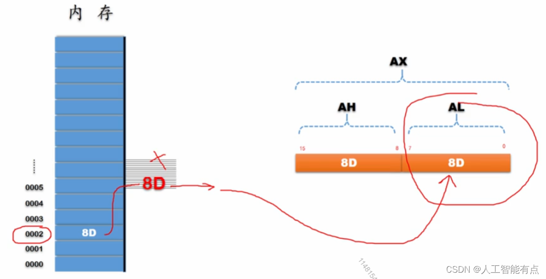
The first four general-purpose registers AXBXCXDX can be split into eight 8-bit registers to provide calculations of 8-bit data. AX split into AHAL. BX split into BHBL. CX split into CHCL. DX is split into DHDL. As shown in the left part of the figure below:
Take a detailed look at how a 16-bit register is split into two 8-bit registers (taking AX as an example):

As can be seen from the figure above, the high 8 bits are the AH register and the low 8 bits are the AL register.
The length of AX is two bytes, one word. (A word is two bytes)
AH and AX are the high-byte part, and AL is the low-byte part of AX.
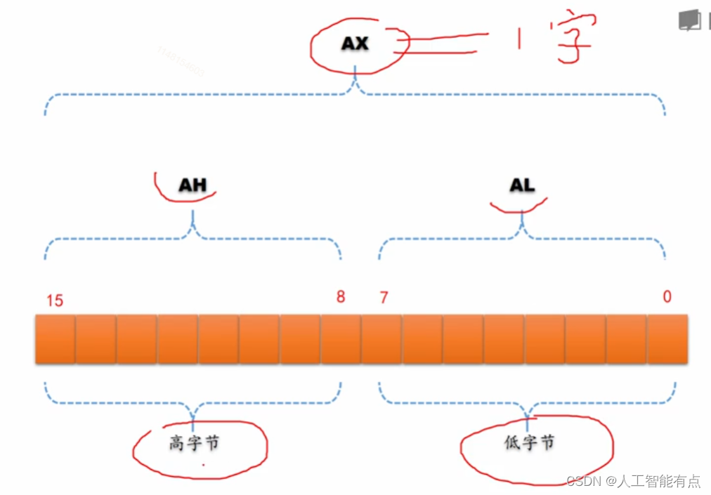
Because AH and AL are split from AX, if the content in AH and AL changes, the content of AX will change accordingly. In other words, they are the same physical hardware, but use different symbols to represent different ranges. When data changes in a small range, data in a large range will inevitably change, because the data is stored in the same place. Therefore, changes in the values of AH and AL affect AX.
2. 8086 memory access and byte order
Intel8086 has 16 data lines, which are the same as the register width. After register C05B reaches the memory through the data line, it is split into two 8-bits, where C0 is the high byte part and 5B is the low byte part. Then, 5B is written into the address unit of 0002, and C0 is written into the address unit of 0003. address unit. The address unit with address bit 0002 is the low address unit, and the address unit with address 0003 is the high address unit.
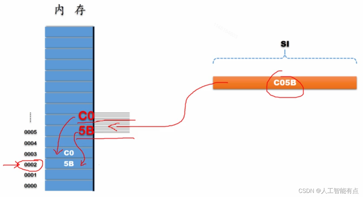
When writing a word, if the low byte is written to the low address unit of the memory, and the high byte is written to the high address unit of the memory, it becomes little endian .
When reading, the same is true. Read a word from address unit 0002 and transfer it to the SI register: because when reading a word, 5B in the low address unit and C0 in the high address unit are taken out and merged into one word C05B on the data line. Finally, it is transferred to the register SI.
Some registers are 8-bit, such as AH and AL. If the content of AH is 8D, write it to memory unit 0002: the length of the register and the memory unit match one byte. The problem is that the width of the data line is 16 bits. When transmitting 8-bit data, only half of the data line is used, and the other half is not used. So, 8D goes into memory half way through the data line and then writes to address cell at memory address 0002. As shown below:
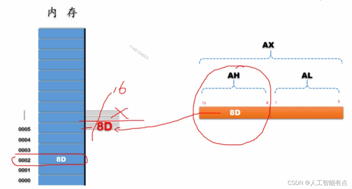
The same is true when reading. AL is read from the memory, read from the 0002 memory unit, and written to AL through half of the data line. As shown below:
3. Program segmentation
3.1 Common noun meanings
If instructions are stored together, they are called code segments .
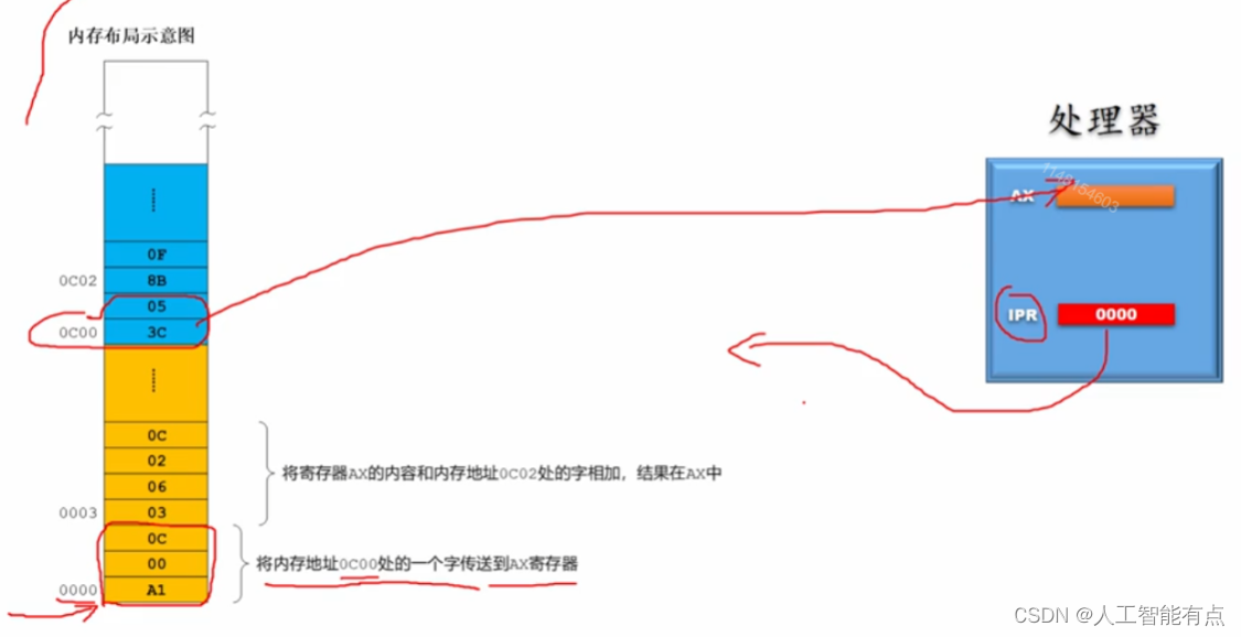
A processor is a device that can automatically fetch and execute instructions. In order to use computers to solve problems we need to program instructions, a process called programming. The result of programming is a program. Look at the picture below:

We have arranged a program in the memory. The program is stored starting from the memory address 0. The processor fetches and executes instructions in order, so the instructions must be stored one by one. In the picture, the yellow part is centralized storage. There are many instructions, but this is just a partial list.
Naturally, these instructions are grouped together to execute the code part of the program, or the instruction part. Because these instructions occupy a continuous section, they are called code segments of the program . The starting address of the code segment here is 0. Data is required when executing instructions, and the data is also stored in memory. In the blue part of the picture, there is a lot of data, and some of them are listed here.
Naturally, the data are gathered together to form the data part of the program. Since these data occupy a continuous section in the memory, we call it the data segment of the program . The starting address of the data segment in the figure is 0c00.
Instructions are composed of opcodes and operands . For the processor, the opcode hides information about how to process the instruction, such as what the instruction does and how to do it.
3.2 Instruction execution process
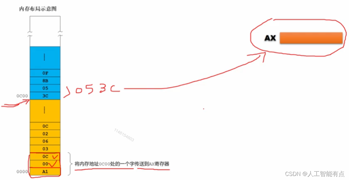
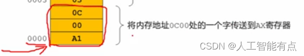
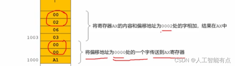
In the picture above, the first instruction is stored starting from address 0, with a total of three bytes. Among them, the first byte A1 is the operation code (implying three pieces of information: first, this is a transfer instruction. Second, the location being transferred is the AX register. Third, the data being transferred is in another location in the memory. One place, the address is 16 bits, immediately after the operation code, because the 8086 processor is low-endian, so this address is 0C00). In short, the function of this instruction is to transfer a word at memory address 0C00 to the AX register. Since the target to be transferred is the AX register, which is 16 bits, the memory is accessed again when this instruction is executed, and a word is obtained from the memory address 0C00. 3C and 05 are combined into 053C, and then passed to the AX register. After the transfer is completed, The content of register AX is 053C.
Let’s look at the second instruction.
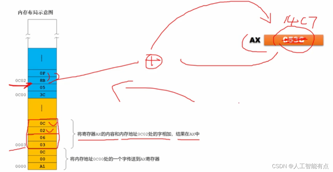
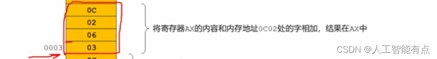
In the picture above, the second instruction is stored starting from memory address 0003, which is four bytes in total. Among them, the first two bytes 03 and 06 are the operation code. Obviously, this operation code is very long and consists of two bytes. The information hidden in opcodes 03 and 06 is (first, this instruction is an addition instruction. Second, the first added number is located in the AX register, and the result of the addition is stored in the AX register. Third, The second added number is located in another place in the memory. Its address is composed of two bytes immediately after the opcode. Here, the two bytes after the opcode are 02 and 0C. , due to 8086 little-endian order, this address is 0C02.). In short, the function of this instruction is to add the contents of register AX to the word at memory address 0C02, and the result is in AX.
4. Program relocation problems
In order to automatically fetch and execute instructions, the processor needs a register to track instructions. Assume its name is IPR. The content of IPR is always the next instruction to be executed. Before the program starts executing, we need to change the first address Transferring to this register, our program starts executing from 0. The address of the first instruction is where the program starts, which is 0. So we transfer 0 to the IPR, and the address of the IPR is now 0. When the program starts executing, the processor puts the contents of the IPR on the address line. The first address issued is 0, so the instruction is fetched from the memory address of 0 and executed. The first fetch is This instruction:
The content of the first instruction is to transfer a word from memory address 0C00 to the AX register. When this instruction is executed, a word is taken from 0C00 and then transferred to the AX register:
At the same time, the content of the register IPR is updated to the address 0003 of the next instruction. Where did this address come from? It's very simple. You can get the address of the next instruction by adding the address of the current instruction and the length of the current instruction. The current instruction address is 0 and the length is 3, so the next instruction address is 3. After the first instruction is executed, the processor uses the contents of the IPR to fetch the second instruction from memory. This is the second instruction:
The content of this instruction is to add the contents of register AX to the word at memory address 0C02, and the result is in AX. When the instruction is executed, the content 0F8B is taken from 0C02 and then added to the content in AX and then written back to AX. At the same time, the contents of the register IPR are automatically updated to the address 0007 (0003+4) of the next instruction.
So far, the program works great. But if the location of the program is changed, will it still work? The following is the program after changing the location (memory address)
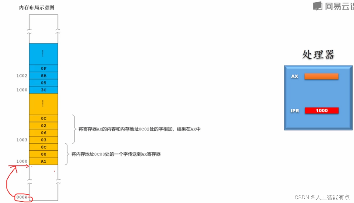
The instructions and data in the program have not changed, but the address of each instruction and each data in the memory has changed. For example: the first address instruction is 0000, and now it is 1000. In order to fetch and execute instructions from the new location, the content of the IPR needs to be updated and set to 1000 before starting execution. This is the new address of the program.
When the program is executed, the processor uses the content of the IPR to issue address 1000 to fetch the first instruction. The content of the first instruction is to transfer a word from the memory address 0C00 to the AX register. However, because the program has just changed the position, that number The address is no longer 0C00 but 1C00, but when this program is executed, it is still taken from the old place 0C00, which is an error. This happens because we use absolute addresses (physical addresses) in memory, such as 0C00 for the first instruction and 0C02 for the second instruction. Such absolute addresses cannot float freely in the memory. In terms of It cannot be relocated.
To solve this problem, you can modify each instruction when the program is loaded to make temporary changes, but this is ridiculous. The instructions of a program can range from dozens to tens of thousands or tens of millions. How to modify so many instructions? Therefore, being able to perform relocation is a basic requirement for the program. There are various programs running in the computer, and the location where each program is loaded at startup is random, and it will be loaded wherever there is free space. Therefore, a good program must be able to float freely in memory without affecting its correct execution, but this requires that we cannot use physical addresses in instructions. So, what should we do?
Introduce segment address and offset address!
5. Segment address and offset address
We solve the program relocation problem by introducing the data segment register
Physical addresses cannot be used in instructions, otherwise the relocation problem cannot be solved. How to solve it?
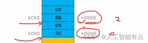
First observe the data segment. The distance between 053C and the starting address of the data segment is 0, so the offset is 0. Look at the distance between 0F8B and the starting address of the data segment is 2 bytes, so the offset of this word from the starting address is 2. For this reason, each word has two attributes, one is the physical address (1C00, 1C02), and the other is the offset relative to the start of the data segment (0 and 2 respectively). From now on, these two The offset of a word relative to its starting address is called the offset address. The "+" in the figure indicates the offset address.
Corresponding modifications are made in the code segment, and the physical address is changed to the offset address.
In order to cope with this change, we added the data segment register DSR in the processor . DSR is used to save the starting address of the data segment.
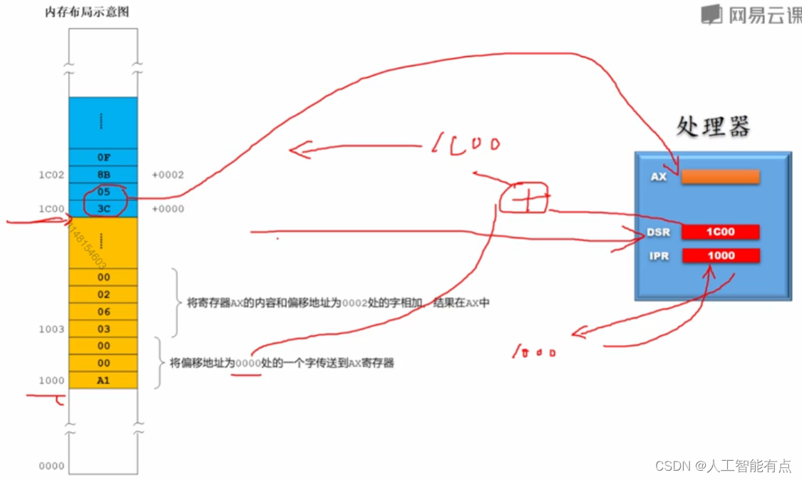
Then, before the program starts executing, the physical address of the first instruction is transferred to the IPR (instruction pointer register). Now the content of the IPR is 1000, and then the actual address 1C00 of the data segment is transferred to the DSR (data segment register). Now The processor starts to fetch and execute instructions: first use IPR to issue 1000 to access the memory and obtain the first instruction. This instruction is to transfer a word at the offset address 0000 to the AX register, which is needed when executing the instruction. Register DSR, at this time, the content 1C00 of DSR is added to the offset address in the instruction to form the physical address 1C00, so the processor sends 1C00 as the address to the memory, then obtains a word 053C from the memory 1C00, and then sends it to AX register. This is the execution process of the first instruction.
At the same time, the content of the register IPR is updated to the address 1003 of the next instruction. After the first instruction is executed, the processor uses the content of the IPR again to send the instruction to the memory at address 1003 to obtain the second instruction. This The content of this instruction is to add the contents of register AX and the word at offset address 0002, and the result is in AX. When the instruction is executed, the segment register DSR needs to be used. At this time, the content 1C00 of the DSR is added to the offset address 002 in the instruction to form the physical address 1C02. Then 1C02 is used to access the memory, and then a word 0F8B is obtained from the memory 1C02. , then add the original contents of 0F8B and AX and send them to the AX register. This is the execution process of the second instruction.
Obviously, after such changes in software and hardware, the program can be placed anywhere in the memory and executed without any modification.
6. 8086 memory access dilemma
Let’s understand the challenges that the INTEL8086 processor faces when accessing memory due to the characteristics of its hardware design.
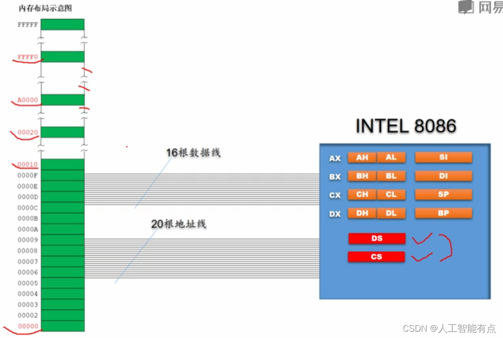
The 8086 has 16 data lines and can access one word of data at a time, which is two bytes of data. The 8086 has 20 address lines. How much memory can it access? 00000-FFFFF.
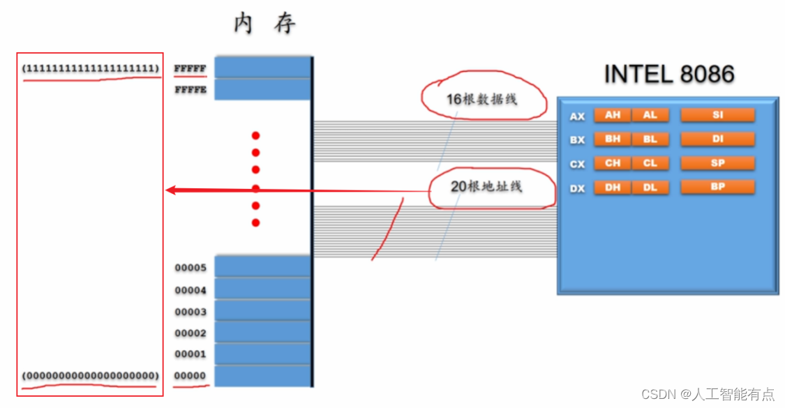
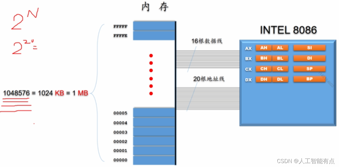
20 address lines can access up to 1048576 units, 1048576 bytes, which is 1MB.
To fetch instructions and data, an address must be issued. The Intel8086 processor integrates registers related to memory access, including the code segment register CS and the data segment register DS.
In principle, the code segment register CS is used to store the starting physical address of the code segment. The address of each instruction can be tracked through the code segment CS, and the processor can use it to automatically fetch and execute instructions.
In principle, the data segment register DS is used to save the starting physical address of the data segment. During the execution of the instruction, the physical address is obtained by adding the content of the data segment DS and the offset address in the instruction. The operand can be obtained through the physical address.
But it is a pity that these registers are 16-bit and cannot accommodate the 20-bit memory address. The 16-bit width register cannot accommodate the address of the 20-bit address line.
How to do it? Breakdown in the next section!
7. 8086 strategy for selecting segment addresses
The code segment register CS and the data segment register DS are used to save the starting addresses of the code segment and data segment. In principle, any memory address can be used as a segment address, but unfortunately, CS and DS are both 16-bit and cannot accommodate There is no 20-digit physical address, but we found that some memory addresses end with 0, such as 00000, 00010, etc., as shown below:
Just imagine, if you remove the 0 at the end of these addresses, the remaining part can be placed in the register, such as FFFF0. If you remove the 0 to FFFF, you can put it in the register CS.
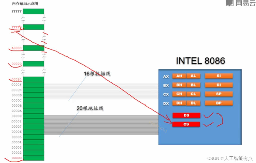
Obviously, in the 8086 system, due to the length limit of the segment register, not all memory addresses can become segment addresses. Only segment addresses ending with 0 can become segment addresses.
For example, if the starting address of the code segment is 30CE0, remove the 0 at the end, and the remaining 30CE can be transferred to CS. The data segment of the program starts at physical address 33CE0, remove 0, and store 33CE in DS. Conversely, when using segment registers to access memory, add the 0 at the end to access the original 20-bit address. In many books, this process is to shift the address to the left by 4 bits or multiply by 16.
According to our original idea, the segment register CS is used to track the physical address of each instruction. For example, the physical address of the first instruction is 30CE0, and the length of the instruction is 3 bytes. During the execution of the first instruction, the processor The content of CS must be modified to the address 30CE3 of the second instruction, but the length of CS is 16 bits and cannot fit the address of the next instruction. This is another problem.
How to get the instruction address in advance? Breakdown in next section.
8. Memory access process of 8086
As mentioned in the previous section, instructions cannot be fetched from the segment register because its width is not enough, only 16 bits. Please consider that although each instruction in the code segment has its physical address, it also has an offset address relative to the beginning of the segment. For example, in this code segment, the offset address of the first instruction is 0000, because it The physical address is the starting address of the code segment. The offset address of the second instruction is 0003, because its offset relative to the code segment is 3 bytes.
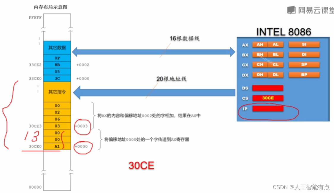
For this reason, the 8086 integrates an instruction pointer register IP , which is specially used to save the offset address of the instruction . Let's follow the execution process of this program to understand how these registers work and how the 8086 fetches and executes instructions.
Before the program starts executing, we need to shift the starting address of the code segment 30CE0 to the right by 4 bits, remove the 0 at the end to get 30CE, and transfer it to the code segment register CS. At this time, the content of the register CS is 30CE. As shown below:
Then the physical starting address of the data segment is shifted to the right by 4 bits, or the 0 at the end is removed to obtain 33CE, and then transferred to the data segment register DS. At this time, the content of DS is 33CE. Finally, we transfer the offset address of the first instruction to the instruction pointer register IP. The content of IP at this time is 0000. As shown below:
At this point, the segment registers all have initial values.
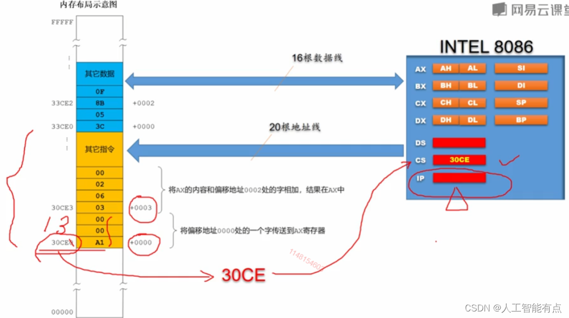
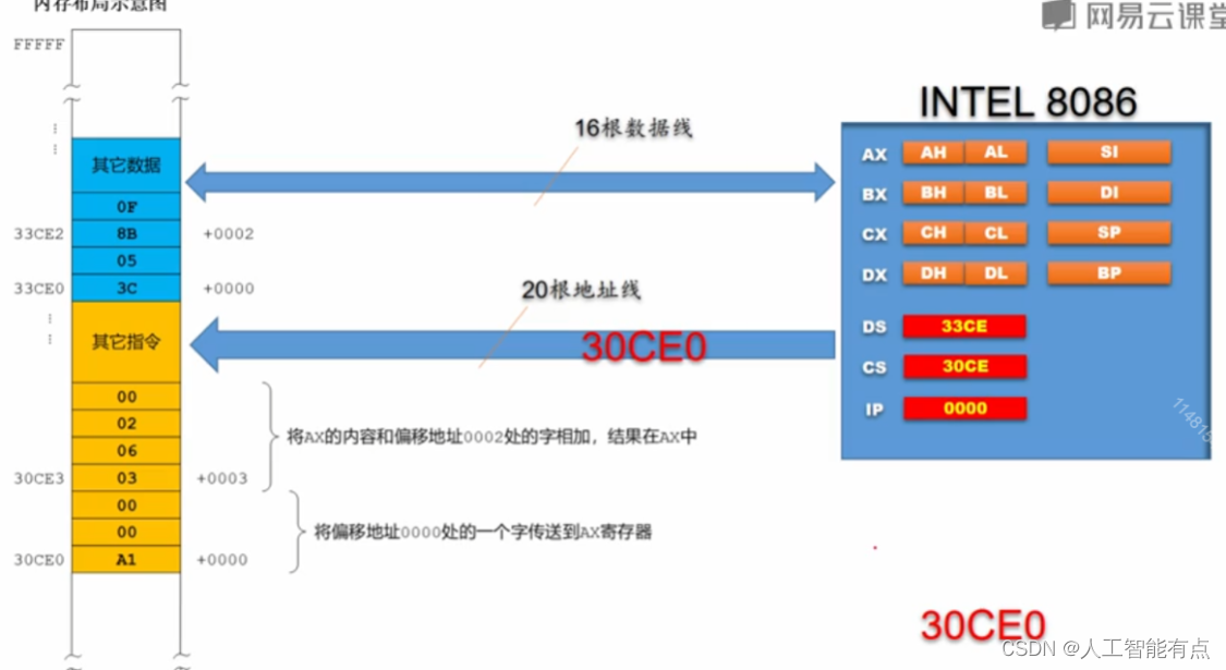
So now the processor starts to fetch instructions, shifts the content of the segment register CS to the left by 4 bits, and gets the 20-bit 30CE0, then adds 30CE0 to 0000 in the instruction pointer register IP, and gets the 20-bit physical address 30CE0, and then adds this The address is sent to the address line to access memory, which will fetch the first instruction at physical address 30CE0 and execute it. This instruction transfers a word at offset address 0000 to the AX register. This will access the memory again. When the instruction is executed, the data segment register DS is required to access the memory. At this time, the content 33CE in DS is shifted to the left by 4 bits to obtain the 20-bit 33CE0, and then 33CE0 is used to compare it with the offset address in the instruction. Added, this will result in a 20-bit physical address 33CE0. As shown below:

Then send this address to the address line to access the memory. This will get a word 053C from the physical address 33CE0, and then send it to the AX register. At the same time, the content of the instruction pointer register IP will be automatically modified to the offset of the next instruction. Address 0003, this number is obtained by using the original number 0000 in IP and adding the length of the first instruction, 3. The content of register IP is now 0003.
After executing the first instruction, the processor enters the instruction fetch stage again, shifts the content of the segment register CS to the left by 4 bits, and obtains the 20-bit number 30CE0, and adds it to the content of the instruction pointer register IP 0003 to obtain the 20-bit number. The address 30CE3 is placed on the address line to access the memory, and the second instruction is obtained from 30CE3 and executed. The content of the instruction is to add the content of AX and the word at offset address 0002 and store it in AX. This will access the memory again. When the instruction is executed, the data segment register DS needs to be used when accessing the memory. At this time, the content of DS is shifted to the left by 4. The bit is 33CE0, which is added to the offset address 0002 to get 33CE2 and sent to the address line to access the memory. The result of adding the contents of 0F8B and AX is taken out from 33CE2 and stored in AX. As shown below:
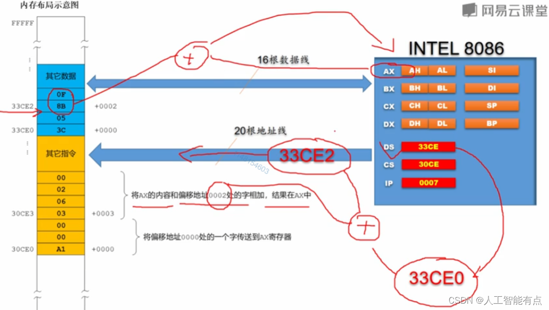
At the same time, the content of the instruction pointer register IP is automatically modified to the offset address 0007 of the next instruction execution. This is obtained by adding the original 3 in IP and the original length of the second instruction.
9. Flexibility of logical addresses and segmentation
Segment register: used to store addresses
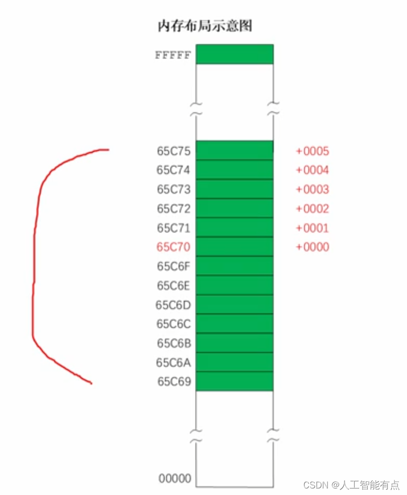
Through the previous description, we already know the principle of 8086 memory segmentation. For example, the following figure shows the addresses of some memory units:
So which of these addresses can be used as the address of 8086? It's okay to end with 0!
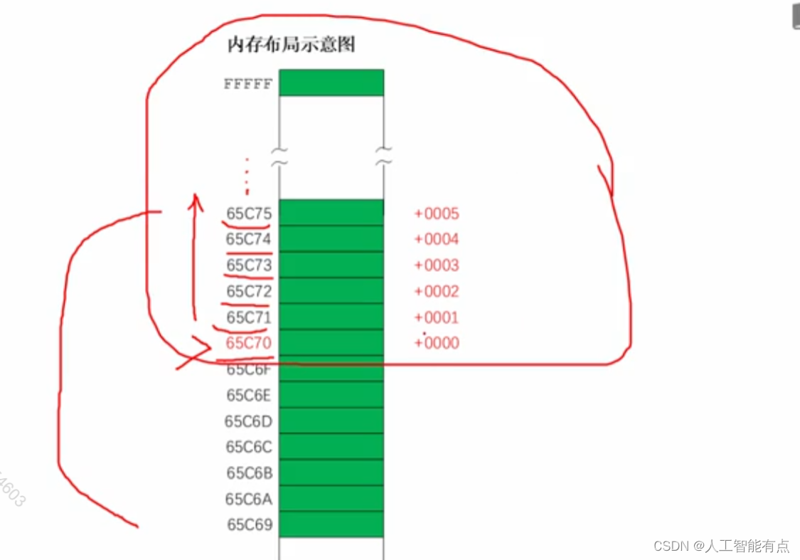
Consider the circle as a segment, then within the segment, the offset addresses of these memory units are 0000 0001 0002 0003 0004 0005. In order to facilitate the description of the relationship between memory unit addresses and segment addresses, a new method of marking memory unit addresses is recommended. Represented as shown below:
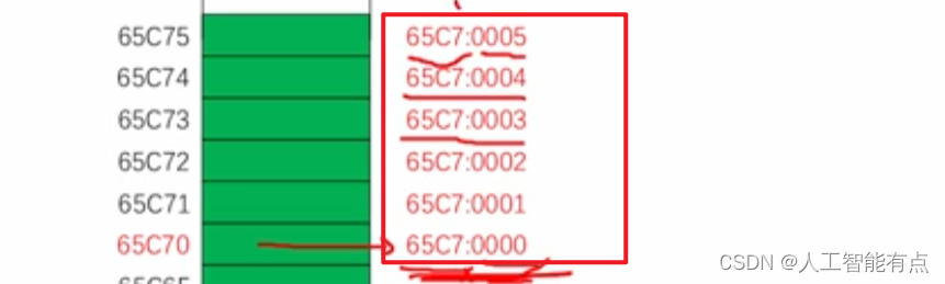
For example, the address of the first memory unit in the segment here is 65C7: 0000, where 65C7 is the segment address with 0 removed from the end (it is a 16-bit segment address), and 0000 after the colon is the offset address within the segment. You can clearly know the starting address and offset address of the segment. This representation is called a logical address.
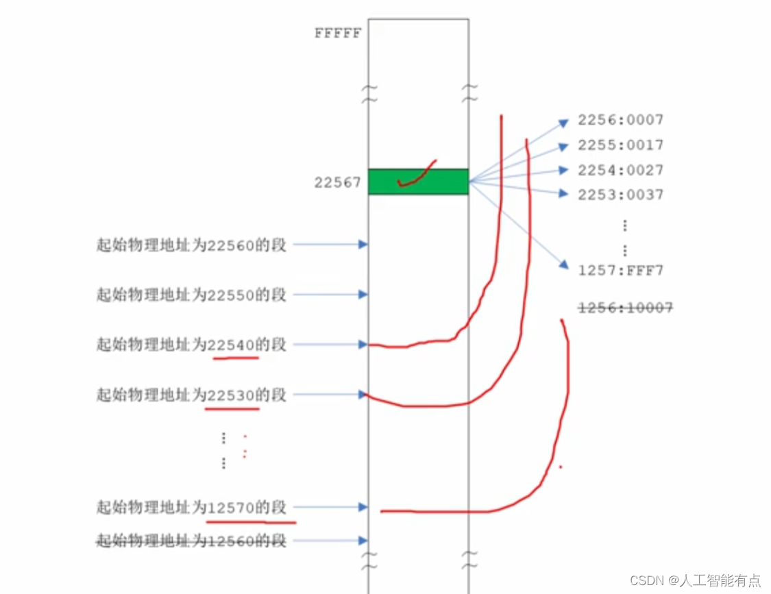
In the 8086 system, to access any memory unit, the segment register is multiplied by 16 to form a 20-bit segment address, and then added to the offset address.
8086 segmentation is very flexible, and one logical address can correspond to multiple physical addresses.
The offset address in 8086 can only be 16 bits, and the maximum is FFFF. 10007 Illegal.
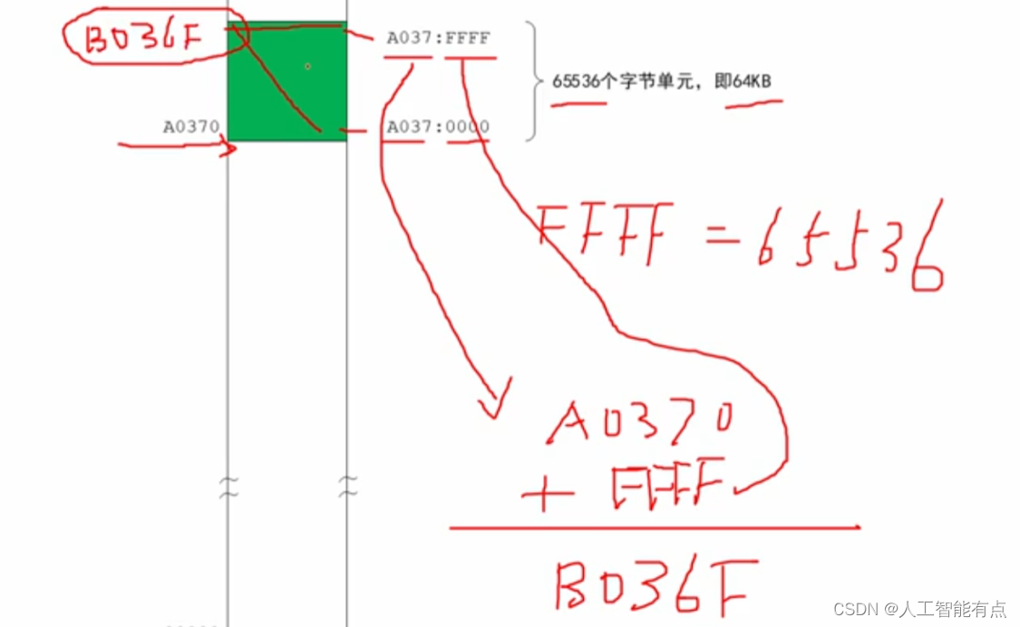
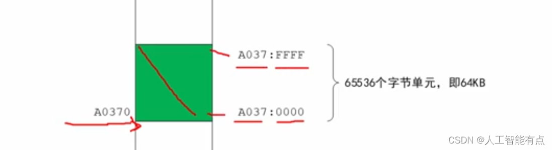
In the previous description, the minimum offset address within the segment is 0 and the maximum is FFFF. So the maximum segment length is 64KB . As shown below:
What is the physical address of the last memory unit in the segment? How to ask for it?
Answer: Multiply the A037 (logical segment address) of the last unit's logical address by 16 and add the logical offset address to get it, as shown below: