Q: Why convert PCB files to GERBER files and drill data?
Answer: Because the GERBER file is an international standard optical drawing format file, it includes two formats, RS-274-D and RS-274-X, among which RS-274-D is called the basic GERBER format, and it must be accompanied by D Only a D code file can completely describe a graphic; RS-274-X is called the extended GERBER format, which itself contains D code information, and commonly used EDA software can generate files in both formats.
Drilling data can also be generated by various EDA software. The general format is Excellon. Drilling data files are very important in the PCB manufacturing process. Without drilling data, PCB boards cannot be drilled, so electrical connections cannot be made, and DIP devices cannot Unable to plug in solder.
Q: Why export the coordinate data, BOM data, and assembly drawings in the PCB file to generate files?
Answer: Because the coordinate data and BOM list data of the device will be lost when the data in the PCB file is converted to the Gerber file, the file needs to be regenerated for production use during the PCBA assembly process.
Altium Designer is a PCB circuit diagram design software. The suffix of the PCB file designed by Altium Designer is PcbDoc. Huaqiu DFM software is a manufacturability and assembly analysis software that can quickly analyze PCB files.
The following is a comparison of the work efficiency of these two software for PCB conversion Gerber, coordinate files, BOM files and assembly drawings.
Steps of converting PCB to production files of AD software
1. Gerber file conversion
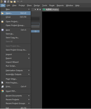
import of files
①FILE→OPEN Find the directory of the file to be loaded
②Drag directly into the software
Set the unit and origin
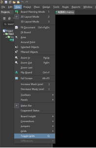
①Setting the unit in the file (usually unit: mil)
Click View-Toggle Units for Chinese-English conversion (or use the shortcut key Q for Chinese-English conversion)
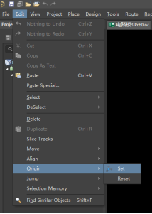
②Edit→Origin→set Set the origin outside the cell border
Soldermask removal for via cap soldermask or plugged vias (when required by customer)
①Drag the original PCB file into AD17 or above version software to open
②Click Design——Rules
③Click Mask——Solder Mask Expansion
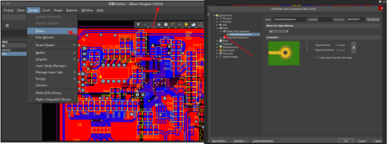
④In the AII box, select the bottom Custom Query
⑤In the pop-up window, click Query Builder
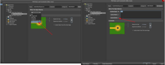
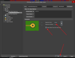
⑥Select Object Kind is——Via
⑦ Check Solder Mask From The Hole Edge and then reduce the window opening by -20mm or -800mil and click OK to output normally
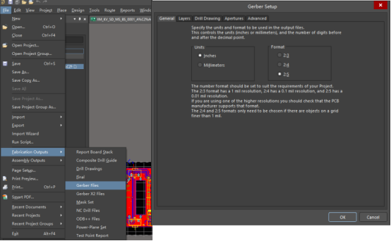
Optical Emoji output
①File→Fabrication Outputs àGerber files
②Select the General item and set the Units and Format (the default option is General), click OK to select the Layers item
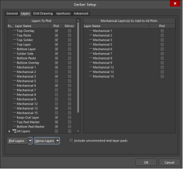
③Pull down Plot Layers and select used ON, pull down Mirror Layers and select ALL OFF, if you want isolated pads in the inner layer, select Include unconnected mid-layer pads, and click OK
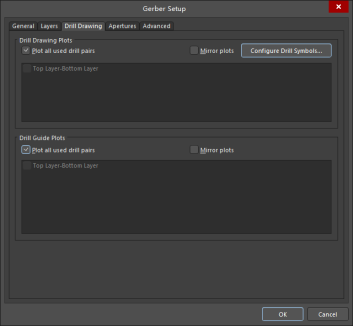
④ Select the Drill Drawing item and the following screen appears, select Plot all used layer pairs, select Plot all used layer pairs, close Mirror plots, close Mirror plots, and click OK
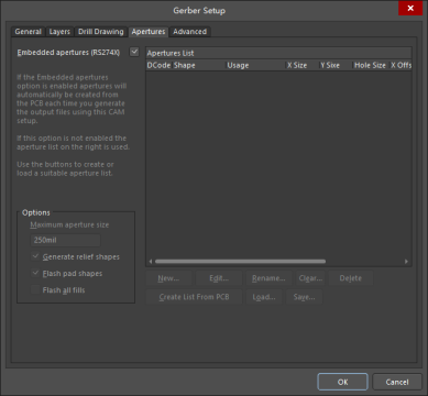
Select the Apertures item and the following screen will appear
①Choose Embedded Apertures (RS274X) as the output GERBER file in D code format
②Click OK
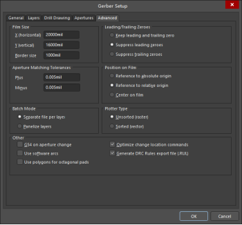
Select the Advanced item and the following screen will appear
①Select G54 on aperture change
②Click OK
③The system automatically outputs the GERBER file to the PCB file, and the system automatically outputs the GERBER file to the PCB file
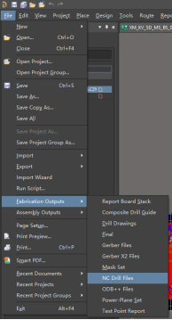
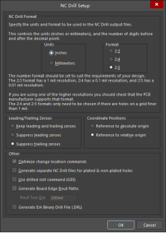
2. Drilling file output
Path Selection
File->Fabrication Outputs->NC Drill Files
Export drill file
Select a good format (the company stipulates 2.4 format, INCHES, TRAILING), click OK and the system will automatically output the drilling file to the directory where the PCB file is located
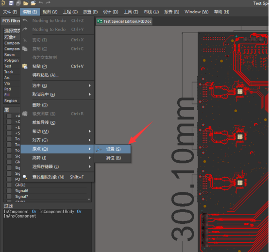
3. Coordinate file export
Set the coordinate reference origin
Open the PCB file, perform (Editl)-(OriginlI)-(Setl), and then click the mouse on the lower left corner of the PCB board
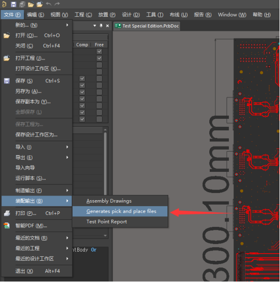
output coordinates file
(File)-(Assembly Outputs)-(Generates pick and place files)
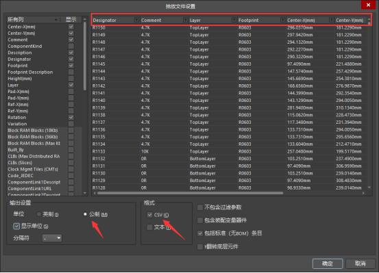
Unit format selection
Next, we can see the output, in which the key bit number (Designator), layer (Layer), package (Footprint), XY coordinates, and angle (Rotation) are very important information, which must contain
Regarding Description and Comment, you can set the output without checking, select the national standard millimeter system as the unit, select .CSV as the format, and click OK.
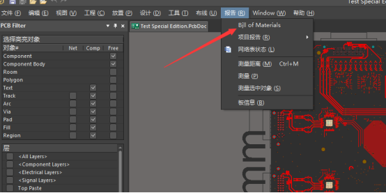
4. BOM file export
open position
Open the Bill of Materials in the report (it can be opened in PcbDoc or SchDoc)
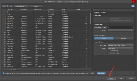
Export BOM file
Click Export on the pop-up window to output the BOM file
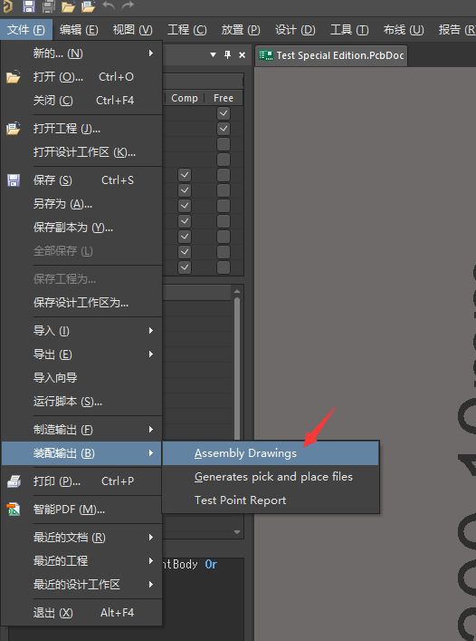
5. Export assembly drawing
Assembly drawing export
Open the Assembly Outputs under the file menu, select the first Assembly Drawings
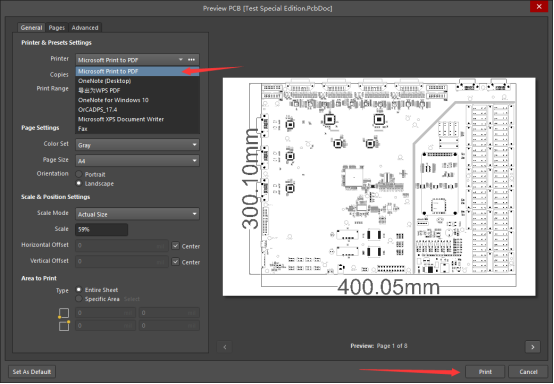
Select output format
Select the output format in Printer, select Microsoft Print to PDF, and click Print to print as a PDF file.
Huaqiu DFM software PCB transfer production file steps
Use Huaqiu DFM software: PCB design files are converted into production files, Gerber, coordinates, BOM files, etc. can be exported directly in the navigation bar with one key, and assembly drawings can also be output with one key, which can be completed in a few seconds.
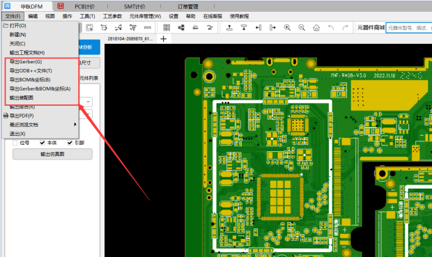
Compared with AD software, Huaqiu DFM software is more efficient in converting production files. See above the files used for Altium Designer software PCB conversion production, at least half an hour or more, Altium Designer is complicated to operate and not everyone can use it, but using Huaqiu DFM software, the operation is simple and efficient, download it quickly to experience more useful function now!