Cached ? Non-Cached?
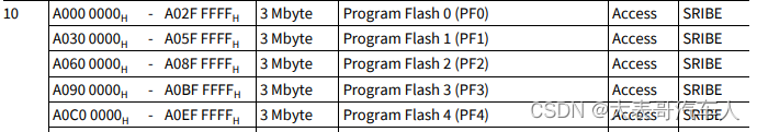
When reading the user manual of TC3XX, in the memory mapping table, two segments are Program Flash, and the size is the same as 3M, and one is segment 8
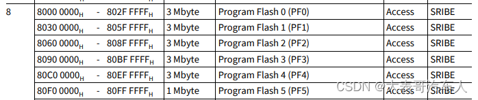
The other is segment10
This inevitably makes people wonder, what is the difference between the two?
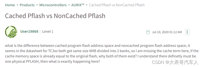
By searching in the infineon developer forum, I found that someone is asking a similar question, and I will analyze the answer to this question.
The same physical flash memory exists in the cache area and the non-cache area. The main difference is how the CPU accesses them.
-
Cache address access : If the CPU accesses the flash memory through the cache address, the acquired data will be stored in the CPU cache. Any subsequent accesses use the data in the cache rather than physically reading the flash memory. This can significantly speed up program execution.
-
Non-cached address access : If the address used is non-cached, then the read operation is always performed physically, that is, the data is read directly from the flash memory every time, without using the CPU cache.
It should be noted that there are certain risks in using the method of caching data. If you change the basic data in the flash memory, but the data in the CPU cache has not been updated, then the CPU will read the old data. This may lead to data inconsistencies. So when dealing with data in flash memory, we need to consider this possible situation and design a correct data synchronization or update strategy.
The comparison of access mechanism between the two and the choice of security mechanism
Learn more about some operations and possible issues with flash reads and writes.
Data Consistency Check
It is best to check on non-cached flash (Non-cached) , because this can ensure that the read operation actually happened. Because if the cache address is used for the read operation, if the data in the flash memory is modified after being read into the cache, the data in the CPU cache will be different from the actual data in the flash memory, which may cause problems.
Writing and erasing of flash memory is done by reflashing. However, write/erase operations are done through command sequences in the DMU (Data Management Unit). So, if the CPU has read data from the flash to its cache, and then some operation reflashes the PFlash, then you will find that the data in the CPU cache is different from the data in the PFlash.
Note that reflash takes a lot of time, so while the code is running, the CPU may try to load other data into the cache, and will notice that the flash memory is not available because it is being changed. The expectation here is that a software programmer doing this will add some checks to the code, but it's also possible that no such checks are done.
Therefore, a well-designed data consistency strategy and proper program checking mechanism are very important when dealing with flash data to prevent problems caused by data inconsistency.
Let's say your security mechanism wants to check the safety of flash data. So if you're running from a cache address, if the data is already in the cache, all you're doing is checking that the cache contents are correct - you're not checking the security of the path to flash itself. You've proven that the path is ok when the data goes into the cache, but you haven't checked what happens afterward. If the data has to be fetched because it's not already in the cache, you're not going to get a speed boost anyway, because you still have to fetch the data.
So to summarize, for a security mechanism, I would use non-cached addresses to make sure that what we are really testing is the security of the path we are interested in.
Choice of Data Security Mechanism
The Data Management Unit (DMU) is used to reprogram the flash memory when needed, so in standard operation it should not be active.
When data is stored in cache, it should be protected with ECC (Error Checking and Correction) (ECC value is stored with data). So when data is read from the cache, the CPU will check the ECC and flag an error if there is a mismatch, so the data in the cache is protected.
ECC is a technique used to detect and correct single data bit errors. When data is stored in the cache, a corresponding ECC value is generated. Then when the data in the cache is read, the ECC will be recalculated and compared with the original ECC value. If there is a mismatch, it means that an error occurred during or during the storage of the data, and the CPU will trigger an error signal.
ESM (Error Signaling Module) is designed to check the contents of PFlash - if you get the contents from the cache, then your security mechanism will no longer test the PFlash, you just re-read the contents of the cache every time, assuming all the data is there .
So if you repeatedly read from the cache, you can see if you have permanent or non-permanent errors in the cache, but you don't mark the PFlash as bad and flush/replace a wordline. To make sure you're really testing PFlash, I think the ESM has to use non-cached addresses. This ensures that you are actually checking if the PFlash itself is corrupted, and you can then use the results to see if you need to replace or flash the flash.
Access Mechanisms to the Cache
Flash memory is physically the same. So when the CPU uses a cache address for a read, it first checks the cache contents, and if it hits, it returns the data from the cache. If there is no hit, it will perform a 256-bit (BTR4) read from PFlash and store the content in the cache. If it's executing a program sequentially, it's likely to read the next 256 bits of data in flash. Also note that PFlash has a prefetch mechanism built in - it fetches the next 256 bits of data, assuming that's what the CPU needs next.
If you access from a non-cached address, then the cache will not be checked, it will be accessed directly from PFlash. However, it fetches the data it needs instead of always doing a BTR4/256 bit read. To maintain performance, PFI (PFlash Interface) will store the 256 bits of data read from PFlash in a local buffer and provide fetches from there until the address goes to the next 256 bits, at which point it will fetch that data (although if there Free prefetch buffer, it may go to fetch the next 256 bits of data).
Whether the CPU continues to step and fetch will depend on the program and what it predicts it will need next.
So the flash memory physically exists in two address spaces at the same time, and the cache is used to improve the access speed of the CPU. However, your security mechanism is to test the actual PFlash, which is why using non-cached addresses is a better idea, because then you can be sure that you are testing what you intend to test. And, by fetching 10 pages, you also ensure that you've flushed every possible buffer and actually returned data from flash.