Software version: vivado 18.3
Chip used: zynq 7020
7020 includes FPGA and ARM. In actual engineering, data transmission can be performed between FPGA and ARM. In this case, joint debugging between PL and PS is required. The process is described below.
1. Add MARK DEBUG
Use the MARK BDBUG statement for ila observation.
First, add (* MARK_DEBUG="true" *) before the signal you want to observe. This part of the statement can be added before the port definition of input or output, as shown in the figure below:
![]()
It can also be added in the following signal declaration, as shown in the figure below:
![]()
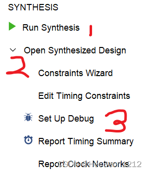
2. Synthesize and set up debug
After adding MARK DEBUG in the .v file, 1. Click Run Synthesis on the left interface of the software; 2. After the Synthesis is completed, expand open synthesis Design; 3. Double-click Set up debug.
The following interface appears
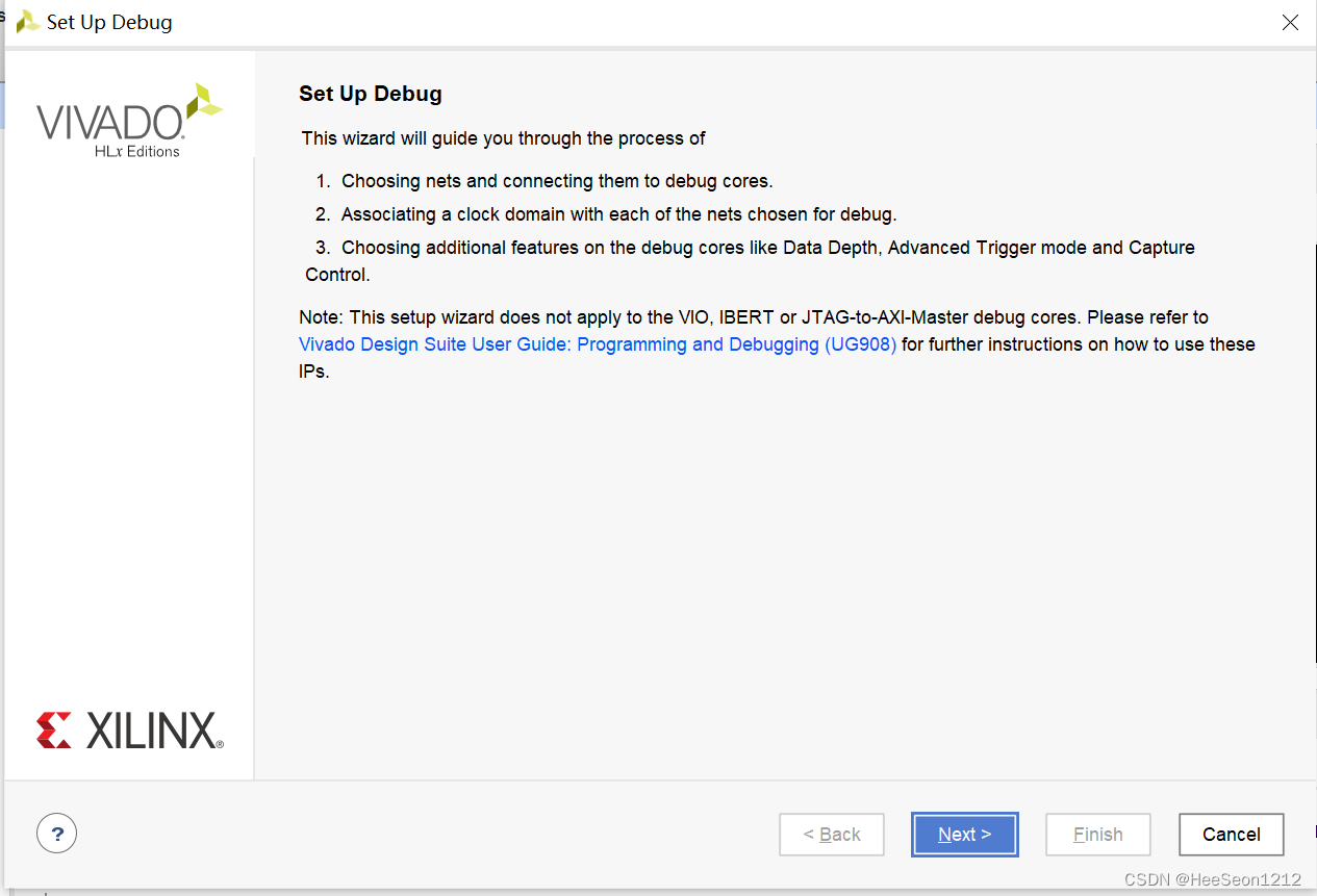
Click next to enter the netlist configuration, NAME is the signal you want to observe, and Clock Domain is the clock domain in which the signal is observed. Select the clock domain of a line to be changed and right click to select the clock domain. Generally, the Clock Domain in a project They are all set to be the same, otherwise it is easy to make mistakes. Pull the progress bar to the right and Driver cell, which is generally the default, and select Data and Trigger for Probe type.
If there is no signal you want to observe in this window, you can add it from netlist by "+". Under normal circumstances, if you have already marked it with MARK DEBUG, this table will contain all the signals you want to observe, and there is no need to add additional ones.


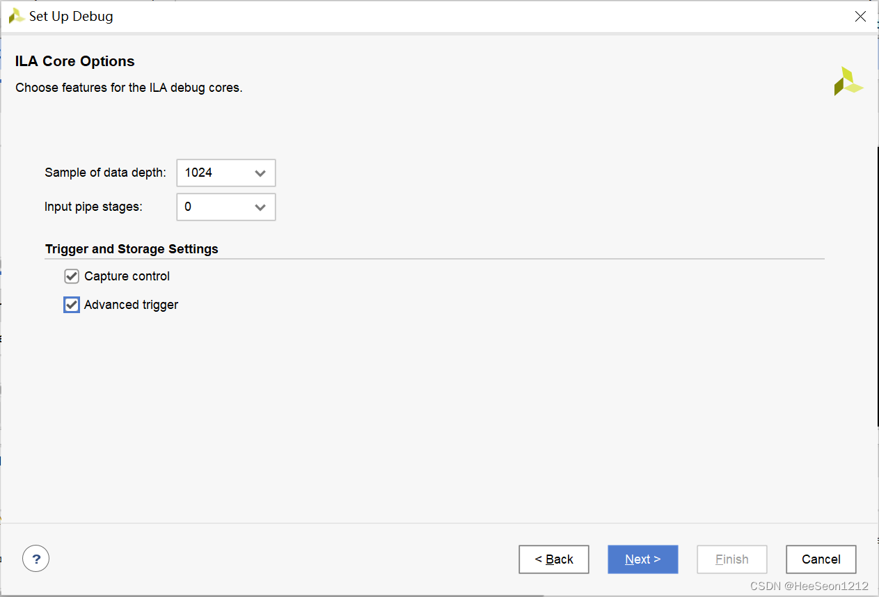
Click next to enter the probe depth configuration, that is, Sample of data depth. The larger the value is selected, the larger the time span of the data that can be seen in the subsequent ila window, which is more conducive to analysis, but if the value is too large, it may There will be a problem of insufficient resources in the implementation later, so try it yourself, remember to check the Capture control and Advanced trigger.
Click next-finish to enter the creating debug core and wait for the generation to end. Schematic will pop up after the generation is complete.

3. Carry out implementation and bit stream generation
Double-click the run implementation on the left interface of vivado, you will be prompted to save the file changes just generated by set up debug, be sure to click save, otherwise the corresponding xdc file is wrong

After saving, click ok all the way and wait for the implementation to complete. The time for this step depends on the complexity of the program.
After completion, click generate bitstream on the left side of the vivado interface and wait for completion.
Do not program the FPGA program after completion, and then program in the SDK to prevent errors in multiple programming phase-locked loops.
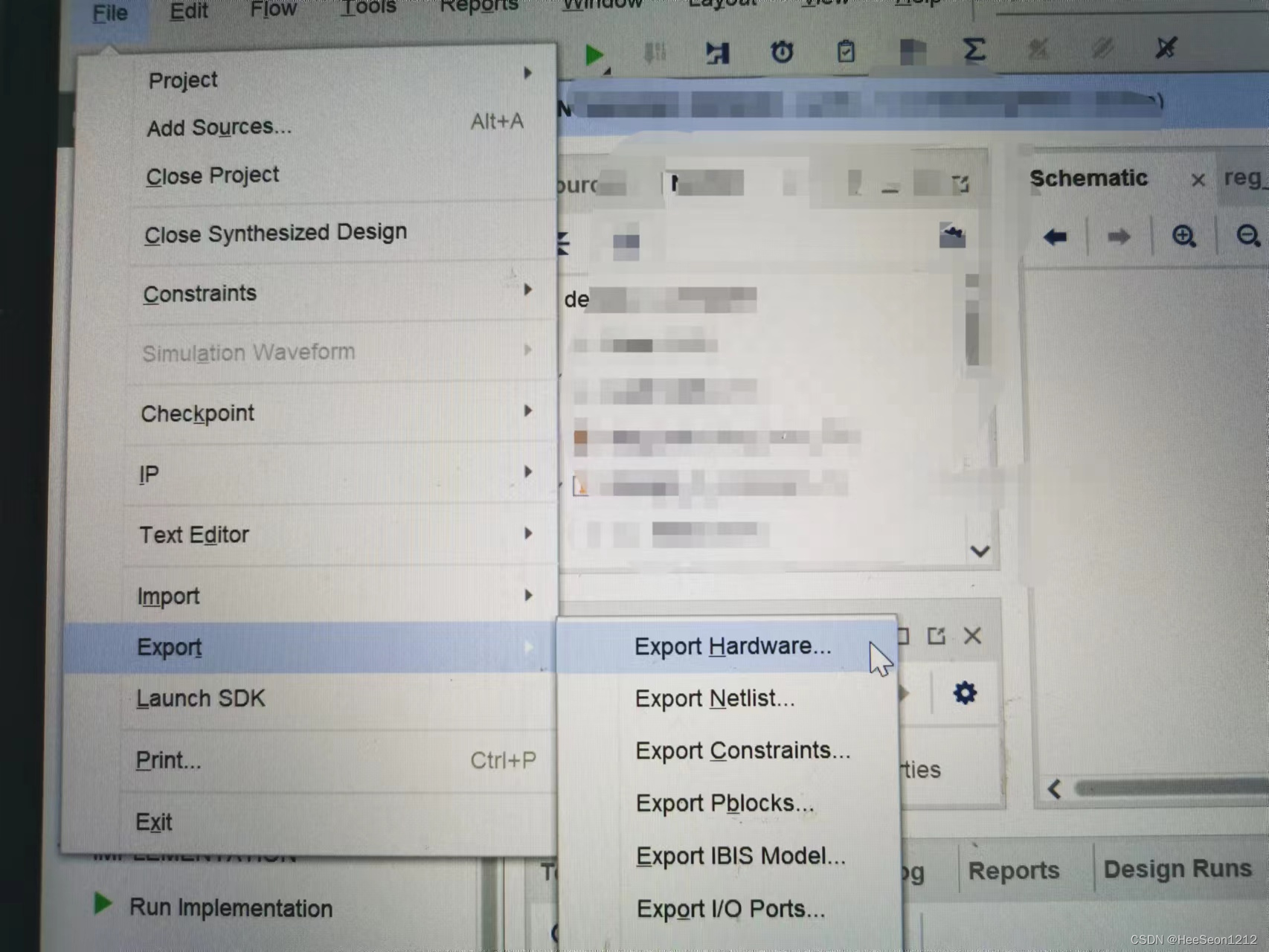
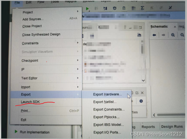
4. Export the hardware platform and open the SDK
After generating the bit stream, click file-export-export hardware in the upper left corner to export the hardware platform, remember to check include bitsream, ok

Then click file-launch SDK in the upper left corner to open the SDK;
Build your project, then select the project in the file directory on the left, right click, select debug as-Debug configuration,

Enter the following interface
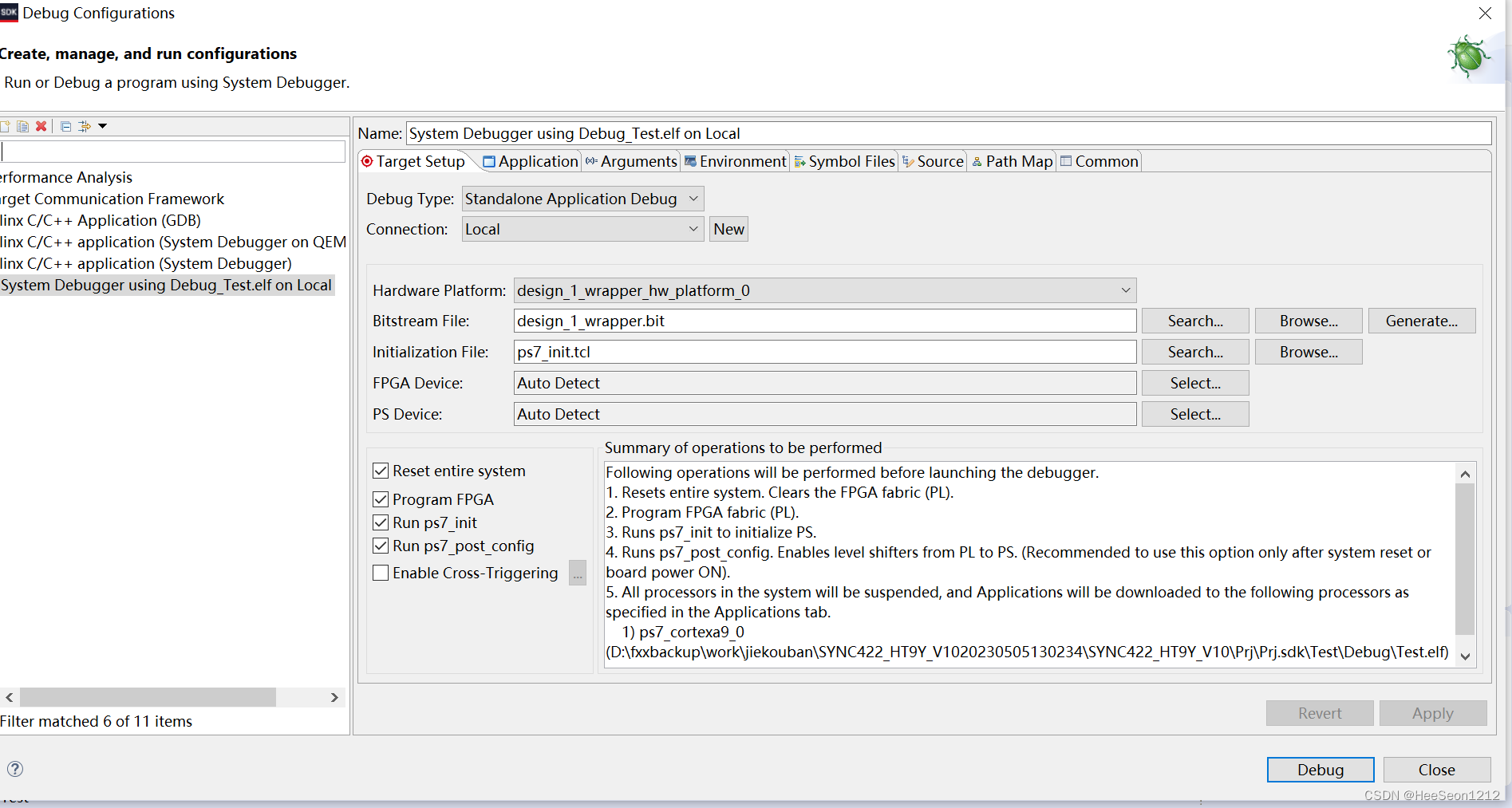
platform, bitstream file select the corresponding file, pay attention to check the Reset entire system and program FPGA, the hardware platform is connected, power on, and then click Debug to enter the normal C language debug mode, at this time you can set breakpoints, Single-step debugging and more.
5. Trigger ila on the FPGA side from the SDK
In the fourth step, the FPGA program has been programmed from the SDK. At this time, the program is already running in the chip.
Return to the vivado interface, click open hardware maneger-click the icon in the red circle, and automatically connect the hardware platform. After connecting the hardware, do not program devices anymore. After a few seconds, the automatic ila observation interface will appear, and you can choose the signal to observe. Set the trigger signal Trigger, etc. Now that I don’t have a board in hand, I won’t take a screenshot.


So far, the PS+PL joint debugging step is over, and the rest is no different from the separate PS debugging and PL debugging.
Can you record the following AXI-LITE communication between PS and PL next time?