References: Altium
Designer PCB Design Common Shortcuts
PCB Shortcuts Settings and Recommendations
1. Setting of shortcut keys
Take the traces in the PCB as an example. First move the mouse to Place→Track, but don't click.
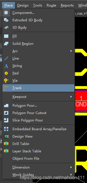
Then hold down Ctrl and click Track with the left mouse button, and the following interface will pop up.
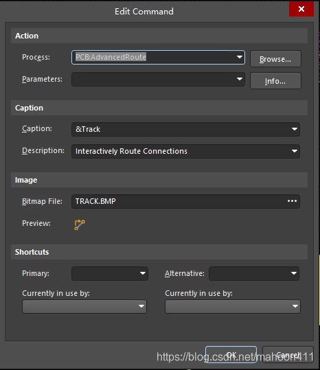
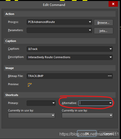
Click the box behind Alternative in Shortcuts.
Here we set the shortcut key of the route to F2, so click F2 on the keyboard, and the above interface becomes the following figure.
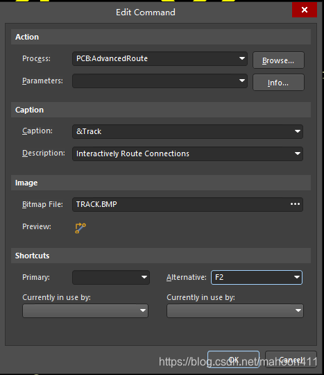
In this way, when routing, press F2 to route.
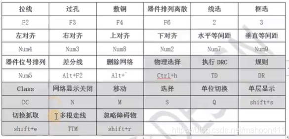
2. Common shortcut keys table
You can refer to the following table and use the above method to set shortcut keys, which is very convenient to use. Among them, the transparent background color is the user-defined shortcut key, and the dark gray background color is the default shortcut key of AD20.
3. Shortcut key conflict resolution
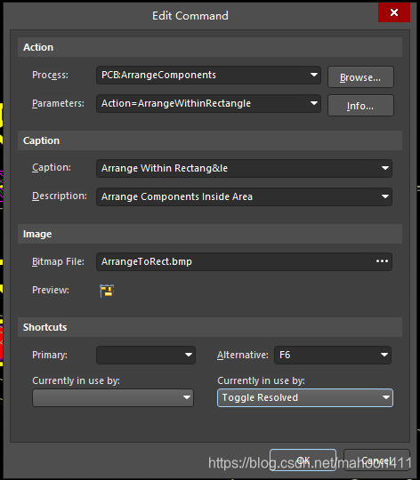
器件排列离散When I set the shortcut keys according to the above table , I encountered a problem that they could not be used after the settings were completed. Later, I found that the shortcut keys could not be used due to the conflict of the shortcut keys. Next, the method to solve the shortcut key conflict is given.
When setting the discrete shortcut keys of the device arrangement, I found that Toggle Resolved is written in Currently in use by in the figure below, indicating that the F6 shortcut key is currently occupied by Toggle Resolved, but we will not use the Toggle Resolved function often, so we only need to use the Toggle Resolved shortcut Press F6 to cancel.
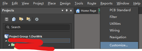
Right-click on the taskbar of the PCB and click Customize.
Click All in the pop-up window.
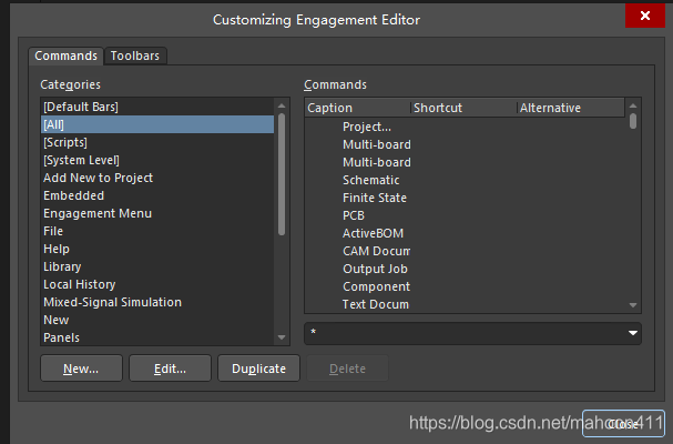
Sort the Shortcuts.

Find the F6 shortcut.
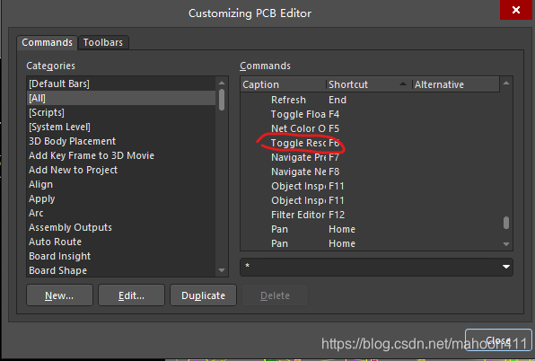
Double-click Toggle Resolved corresponding to F6 to enter the shortcut key setting page
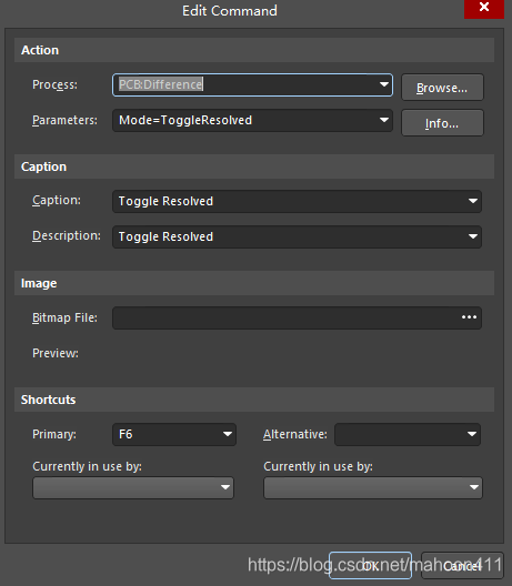
Change the F6 after Primary in Shortcuts to None, and you're done.

Use the F6 shortcut key again to realize the discrete function of device arrangement.
4. Common shortcut keys for other PCB defaults
The following are the default shortcut keys of AD, which can be used directly without additional settings.
| button | Function |
|---|---|
| A | Align menu |
| D | design menu |
| E | Edit menu |
| J | Jump menu |
| M | mobile menu |
| N | Show/hide nets and flying leads |
| Q | Unit switching (switch to mil or mm) |
| S | option menu |
| T | Tools menu |
| V | View menu |
| 2/3 | Keyboard number 2 can switch 2D display, .3 is to switch 3D display |
| Combination keys | Function |
|---|---|
| A+A | Like the schematic, go to the alignment options |
| Ctrl+left click | Highlight and click the target and the connected network (you can adjust the brightness by pressing [ ] on the keyboard) |
| Ctrl+G | Open grid settings |
| Ctrl+H | physical choice |
| Ctrl+M | Point-to-point measurement (that is, measuring distance) |
| D+C | Open Object Class Browser |
| D+S+D | Quickly define a board frame with the board frame selected |
| D+P | Generate a PCB library (in short, get the package of the PCB) |
| D+K | Open the Cascade Manager |
| D+R | Open Rules Manager (Design Rules) |
| E + K | Break the wire bridge (similar to dividing a signal wire into multiple segments optional) |
| E + A | Special pasting (you can choose array pasting, choose circular or linear, and can also be used when drawing and changing device package pins) |
| E + D | Click to delete (click the network cable with the left mouse button to quickly delete a single network cable) |
| E+O+S | Set the origin (that is, set the origin of the PCB coordinate axis) |
| G+G | Grid size settings |
| D+C | jump to device |
| L | Open the visualization configuration, you can set which layer to display |
| M+S | mobile selection |
| P+V | Place vias (you can use the Tab key to modify the properties) |
| P+T | place wire |
| P+P | place pads |
| P+S | Place strings (you can also modify properties through Tab, similar to placing network labels) |
| R+M | Measure distance (same as above) |
| S+L | Line selection (select devices through a line, easy to operate, similar to the selection of multiple lines) |
| S+N | choose network |
| shift+S | Single-layer display (only one layer is displayed, ignoring the visual distraction of other layers) |
| Shift+C | Clear filter (that is, the clear button of the graphical interface, generally after finding the device through the cross probe, you can use this to contact the status) |
| Shift+E | Toggle Hot Scraping |
| Shift+F | Find similar objects (you can quickly modify the device with this operation) |
| Shift+R | Switch routing mode |
| Shift+H | Turn on/off the head-up display (that is, to display the coordinate axis information and layer information in the upper left corner of the PCB) |
| Shift+W | Switch between different trace widths (this needs to be operated under the condition of traces, quickly modify the line width, if you cannot modify it, please go to the rules to check the maximum line width) |
| Shift+Space | Switch the routing direction |
| T+E | Place teardrops (increase the contact between the pad and the signal line) |
| T+C | Cross-probe (you can quickly find the position of the device in the PCB on the schematic by this operation) |
| T+M | Reset DRC error (many students do not operate standardly during design, and there is no design rule, which will lead to green color during PCB layout, similar to 51 MCU putting the crystal into the MCU, you can press T+M to ignore the error by default) |
| T+P | Open the system parameter settings (you can set the number of undos, the angle that the device rotates by space each time, and other settings) |
| V+B | flip the board |
| V+F | The view is suitable for the board (you can quickly locate the interface suitable for your own board) |
| V+D | Appropriate design of the view (similar to the above, one big and one small) |
| V + S | Open/close the Panel panel (that is, to open and close the unit display and some other operation menu bars below, it is generally recommended to keep it) |
| T+D | Turn on rule detection (you can turn off rule detection in it, so that the crystal oscillator will not report green when placed in the microcontroller before) |
| T+D+R | Run DRC detection (don't use this if the general rules are not designed) |
| Numpad +/- | switch layer |