Series of articles catalog
Base element 1.
The circuit design 3.PCB design 4. The welding element 6. programming 9. testing standards
Article Directory
Preface
For those who can’t find the direction of struggle after graduating from university (updated from time to time every week)
embedded system designer exam
1. "Ground" on the PCB
1. Detailed explanation of single-point grounding, multi-point grounding, and mixed grounding in circuit design
The ground wire is also impedance. When current flows through the ground wire, a voltage will be generated. This is a noise voltage, and the noise voltage is one of the interference sources that affect the stability of the system, which is undesirable. Therefore, the prerequisite for reducing ground noise is to reduce the impedance of the ground wire.
As we all know, the ground wire is the path for the current to return to the source. For a signal, it needs to find a path for the lowest impedance current to return to the ground, so how to deal with this signal return becomes very critical. First, according to the formula, it can be known that the radiation intensity is proportional to the loop area, that is, the longer the path that reflow needs to take, the larger the loop formed, and the greater the interference with external radiation. Therefore, when the PCB is laid out It is necessary to reduce the area of the power circuit and signal circuit as much as possible. Second, for a high-speed signal, providing good signal return can ensure its signal quality. This is because the characteristic impedance of the transmission line on the PCB is generally calculated based on the ground layer (or power layer). There is a continuous ground plane nearby so that the impedance of this line can remain continuous. If there is no ground reference near a segment of the line, the impedance will change. Discontinuous impedance will affect the integrity of the signal. Therefore, when wiring, the high-speed line should be allocated to the layer close to the ground plane, or one or two ground lines should be walked beside the high-speed line to play the function of shielding and providing nearby return. Third, why do we try not to split across the power supply when wiring? This is also because after the signal crosses different power layers, its return path will be very long and it will be easily interfered. Of course, it is not strictly required that the power supply cannot be divided. It is possible for low-speed signals, because the interference generated can be ignored compared to the signal. For high-speed signals, check carefully and try not to cross over. You can adjust the wiring of the power supply part.
Many electromagnetic interference problems are caused by the ground wire, because the ground wire potential is the reference potential of the entire circuit. If the ground wire is not designed properly, the ground wire potential is unstable, which will cause the circuit to malfunction. The purpose of ground wire design is to ensure that the ground wire potential is as stable as possible to eliminate interference. There are generally three signal grounding methods: floating ground, single-point grounding, multi-point grounding, and mixed grounding.
A. Floating ground
Purpose: Isolate the circuit or equipment from the common ground wire that may cause circulating current. Floating ground also makes it easy to coordinate between circuits of different potentials. Disadvantages: It is easy to accumulate static electricity and cause strong electrostatic discharge. A compromise solution: connect a bleeder resistor.
B. Single point grounding
Single-point grounding: The ground wires of all circuits are connected to the same point of the common ground wire, which can be further divided into series single-point grounding and parallel single-point grounding. Do not use it in a system where high-power and low-power circuits are mixed, because the ground current in the high-power circuit will affect the normal operation of the low-power circuit. In addition, the most sensitive circuit should be placed at point A, where the potential is the most stable. The biggest advantage is that there is no ground loop, which is relatively simple, but the ground wire is often too long, resulting in excessive ground wire impedance.

Single-point grounding can be divided into "series grounding" and "parallel grounding" two ways. The way of single-point grounding in series is simple, but there is a common ground wire, which leads to the existence of a common ground wire impedance. If a circuit with a large power difference is connected in series at this time, the mutual interference will be very serious. Parallel single-point grounding can avoid the common ground wire coupling factor, but each part of the circuit needs to lead the ground wire to the grounding point, which requires too many ground wires, which is not practical.
Therefore, in actual application, the PCB board can be drawn to adopt a single-point grounding method of a combination of series and parallel. At that time, put the circuits that are not easy to interfere with each other on one layer, put the circuits that easily interfere with each other on different layers, and then connect the grounds of different layers in parallel to ground. As shown below.

Single-point grounding is used for low operating frequency (<1MHz).
Disadvantage: Not suitable for high-frequency applications.
Single-point grounding is in a high-frequency circuit. Because the ground wire is long and the impedance of the ground wire is a factor that can never be avoided, it is not applicable. What should I do? "Multi-point grounding" will be introduced below.
C. Multi-point grounding
The high working frequency (>30MHz) adopts the multi-point grounding type (that is, in the circuit system, a grounding plate is used to replace the respective ground loops in each part of the circuit). Because the inductance of the ground lead is proportional to the frequency and length, the common ground impedance will increase when the operating frequency is high, which will increase the electromagnetic interference generated by the common ground impedance, so the length of the ground wire is required to be as short as possible. When using multi-point grounding, try to find the nearest low-resistance ground plane to ground. High-frequency digital circuits need to be grounded in parallel, and it is generally easier to handle them here by way of ground holes.
When the working frequency of the circuit is high, imagine how severe the impact on the surrounding circuits will be when the high-frequency signal propagates along the ground wire. Therefore, all circuits must be connected to the ground nearby. The ground wire requires the shortest and more points. Grounding occurs.
The purpose of multi-point grounding is to reduce the impedance of the ground wire. In the high frequency (under certain conditions of f) circuit, to reduce the impedance, there are two main considerations. One is to reduce the resistance of the ground wire, and the other is to reduce the impedance of the ground wire. Small ground wire inductive resistance.
Methods as below:
1. Reduce the resistance of the ground conductor. From the formula of the relationship between resistance and cross section, we know that the cross-sectional area of the ground conductor should be increased. However, in the high-frequency environment, there is a skin effect of high-frequency current (also called skin effect), and high-frequency current will pass on the surface of the conductor, so simply increasing the cross-sectional area of the ground conductor is often not effective. You can consider plating silver on the surface of the conductor, because the conductivity of silver is better than other conductive materials, so it will reduce the conductor resistance.
2. The best way to reduce the inductive reactance of the ground wire is to increase the area of the ground wire.
In practical applications, the ground wire is short and the ground area is large, and the anti-interference effect will be better.
At the time of writing, some people may ask, what is a high-frequency circuit? Refer to Professor Yang Jishen’s book "Electromagnetic Compatibility EMC Technology", it is mentioned that "usually 1MHZ is considered a low-frequency circuit and can be grounded at a single point, and a high-frequency circuit above 10MHZ can be used for multi-point grounding." At 1MHZ and 10MHZ, if The longest ground wire does not exceed 1/20 of the wavelength, and it can be grounded at a single point, otherwise it can be grounded at multiple points.

What if there are both high-frequency signals and low-frequency signals in the circuit? Hybrid grounding would be a good choice!
D, mixed grounding
as the picture shows.

Analyze through the figure: The first structure in the above figure assumes that it works in a low-frequency circuit. According to the capacitive reactance Zc = 1/2πfc, it can be known that the capacitive reactance is very large in a low-frequency environment, but very small in a high-frequency environment. Then the ground wire is disconnected at low frequencies and is close to conducting when subjected to high frequency interference. This connection method can effectively avoid the interference effect of the ground loop.
The second structure in the above figure assumes that it works in a high-frequency circuit. According to the inductive reactance Zl = 2πfl, it can be seen that the inductive reactance is very small in a low-frequency environment, but very large in a high-frequency environment. Then the ground wire is similarly conductive at low frequency and disconnected when subjected to high frequency interference. This connection can effectively avoid the influence of ground loop current.
If you do not choose to use the entire plane as a common ground wire, for example, when the module itself has two ground wires, you need to divide the ground plane, which often interacts with the power plane. The connection method between the grounds is as follows:
① Common wiring connection of circuit board between grounds: This method can ensure reliable low-impedance conduction between the two ground wires, but it is limited to the connection between the medium and low frequency signal circuit grounds.
② Large resistance connection between the ground: The characteristic of a large resistance is that once a voltage difference appears across the resistor, a very weak conduction current will be generated. After the charge on the ground line is discharged, the voltage difference between the two ends will eventually be zero.
③ Capacitor connection between grounds: Capacitors are characterized by DC cut-off and AC conduction, and are used in floating systems.
④ 地间磁珠连接:磁珠等同于一个随频率变化的电阻,它表现的是电阻特性。应用于快速小电流波动的弱信号的地与地之间。
⑤ 地间电感连接:电感具有抑制电路状态变化的特性,可以削峰填谷,通常应用于两个有较大电流波动的地与地之间。
⑥ 地间小电阻连接:小电阻增加了一个阻尼,阻碍地电流快速变化的过冲;在电流变化时候,使冲击电流上升沿变缓。
2模拟地和数字地
模拟信号和数字信号都要回流到地,因为数字信号变化速度快,从而在数字地上引起的噪声就会很大,而模拟信号是需要一个干净的地参考工作的。如果模拟地和数字地混在一起,噪声就会影响到模拟信号。一般来说,模拟地和数字地要分开处理,然后通过细的走线连在一起,或者单点接在一起。总的思想是尽量阻隔数字地上的噪声窜到模拟地上。
3星型接地
“星型"接地的理论基础是电路中总有一个点是所有电压的参考点,称为"星型接地"点。我们可以通过一个形象的比喻更好地加以理解—多条导线从一个共同接地点呈辐射状扩展,类似一颗星。星型点并不一定在外表上类似一颗星—它可能是接地层上的一个点—但星型接地系统上的一个关键特性是:所有电压都是相对于接地网上的某个特定点测量的,而不是相对于一个不确定的"地”。
4屏蔽层如何接地
屏蔽电缆的屏蔽层、信号包地都要接到单板的接口地上而不是信号地上,这是因为信号地上有各种的噪声,如果屏蔽层接到了信号地上,噪声电压会驱动共模电流沿屏蔽层向外干扰,所以设计不好的电缆线一般都是电磁干扰的最大噪声输出源。
综述,在实际应用中,电路根据工作环境采用合适的接地方式可以有效避开干扰信号,达到电路的最优效果。
二、信号
1.PCB设计中高速信号与低速信号的区分
出处:搜狐
在PCB设计中,如何区分高速信号与低速信号?很多人有一个误区,一般认为频率高的信号就是高速信号,对于GHz这样的信号来说无可厚非,但却不能一概而论。
我们来看看Cadence公司对高速信号的判断:
凡是大于50MHz的信号,就是高速信号;
信号是否高速和频率没有直接关系,而是信号上升/下降沿小于50ps时就认为是高速信号;
当信号所在的传输路径长度大于1/6λ,信号被认为是高速信号;
当信号沿着传输路径传输,发生了严重的趋肤效应和电离损耗时,被认为是高速信号。
所以说高速信号并不是以频率高低来界定的,那么应该怎样区分高低速信号呢?
在高速信号的设计中,一般考虑的并不是信号的周期频率F,一般是有效频率F1,T代表信号的时钟周期,T1代表信号的10%-90%的上升时间,则有:
周期频率定义:F=1/T
有效频率定义:F1=0.5/T1
低速信号中,各个点的电平相差不大,但高速信号中,需要用分布式的思维来考虑问题,在传输路径中,每个点的路径相差很大,所以高低速信号的划分还与信号的传输路径有关。
信号的传输长度小于信号波长的1/6时,可认为是低速信号,反之高速。λ是信号波长,c是信号在PCB上传输速度,F是信号的有效频率。
λ=c/F
在C为常数的情况下,λ与F成反比,即频率F越高,波长越短,可以划分的高低速信号线的分水的线长越短。
总结:高速信号与低速信号的区分方法
1、获得有效频率F1及走线长度L
2、利用有效频率F1计算信号的波长λ
3、判断L与1/6*λ的大小关系,L大为高速信号,反之为低速。
补充:一般有效频率可以由专业仪器测量得到,也可以估算,可假设上升沿为信号周期的7%,假如信号频率是10MHz,可以假设有效频率是70MHz。
三、噪声
1.PCB设计中高速信号与低速信号的区分
原文出处
随着IC 器件集成度的提高、设备的逐步小型化和器件的速度愈来愈高,电子产品中的EMI问题也更加严重。从系统设备EMC /EMI设计的观点来看,在设备的PCB设计阶段处理好EMC/EMI问题,是使系统设备达到电磁兼容标准最有效、成本最低的手段。本文介绍数字电路PCB设计中的EMI控制技术。
1 EMI的产生及抑制原理
EMI的产生是由于电磁干扰源通过耦合路径将能量传递给敏感系统造成的。它包括经由导线或公共地线的传导、通过空间辐射或通过近场耦合三种基本形式。EMI的危害表现为降低传输信号质量,对电路或设备造成干扰甚至破坏,使设备不能满足电磁兼容标准所规定的技术指标要求。
为抑制EMI,数字电路的EMI设计应按下列原则进行:
●根据相关EMC/EMI技术规范,将指标分解到单板电路,分级控制。
●从EMI的三要素即干扰源、能量耦合途径和敏感系统这三个方面来控制,使电路有平坦的频响,保证电路正常、稳定工作。
●从设备前端设计入手,关注EMC/EMI设计,降低设计成本。
2 数字电路PCB的 EMI控制技术
在处理各种形式的EMI时,必须具体问题具体分析。在数字电路的PCB设计中,可以从下列几个方面进行EMI控制。
2.1 器件选型
在进行EMI设计时,首先要考虑选用器件的速率。任何电路,如果把上升时间为5ns的器件换成上升时间为2.5ns的器件,EMI会提高约4倍。EMI的辐射强度与频率的平方成正比,最高EMI频率(fknee)也称为EMI发射带宽,它是信号上升时间而不是信号频率的函数:fknee =0.35/Tr (其中Tr为器件的信号上升时间)
这种辐射型EMI的频率范围为30MHz到几个GHz,在这个频段上,波长很短,电路板上即使非常短的布线也可能成为发射天线。当EMI较高时,电路容易丧失正常的功能。因此,在器件选型上,在保证电路性能要求的前提下,应尽量使用低速芯片,采用合适的驱动/接收电路。另外,由于器件的引线管脚都具有寄生电感和寄生电容,因此在高速设计中,器件封装形式对信号的影响也是不可忽视的,因为它也是产生EMI辐射的重要因素。一般地,贴片器件的寄生参数小于插装器件,BGA 封装的寄生参数小于QFP 封装。
2.2 连接器的选择与信号端子定义
连接器是高速信号传输的关键环节,也是易产生EMI的薄弱环节。在连接器的端子设计上可多安排地针,减小信号与地的间距,减小连接器中产生辐射的有效信号环路面积,提供低阻抗 回流通路。必要时,要考虑将一些关键信号用地针隔离。
2.3 叠层设计
在成本许可的前提下,增加地线层数量,将信号层紧邻地平面层可以减少EMI辐射。对于高速PCB,电源层和地线层紧邻耦合,可降低电源阻抗,从而降低EMI。
2.4 布局
根据信号电流流向,进行合理的布局,可减小信号间的干扰。合理布局是控制EMI的关键。布局的基本原则是:
●模拟信号易受数字信号的干扰,模拟电路应与数字电路隔开;
●时钟线是主要的干扰和辐射源,要远离敏感电路,并使时钟走线最短;
●大电流、大功耗电路尽量避免布置在板中心区域,同时应考虑散热和辐射的影响;
●连接器尽量安排在板的一边,并远离高频电路;
●输入/输出电路靠近相应连接器,去耦电容靠近相应电源管脚;
●充分考虑布局对电源分割的可行性,多电源器件要跨在电源分割区域边界布放,以有效降低平面分割对EMI的影响;
●回流平面(路径)不分割。
2.5 布线
●阻抗控制:高速信号线会呈现传输线的特性,需要进行阻抗控制,以避免信号的反射、过冲和振铃,降低EMI辐射。
●将信号进行分类,按照不同信号(模拟信号、时钟信号、I/O信号、总线、电源等)的EMI辐射强度及敏感程度,使干扰源与敏感系统尽可能分离,减小耦合。
●严格控制时钟信号(特别是高速时钟信号)的走线长度、过孔数、跨分割区、端接、布线层、回流路径等。
●信号环路,即信号流出至信号流入形成的回路,是PCB设计中EMI控制的关键,在布线时必须加以控制。要了解每一关键信号的流向,对于关键信号要靠近回流路径布线,确保其环路面积最小。
2.PCB板层布局与EMC
四、AD的使用
1.Altium Designer的PCB中ROOM的功用、放置、修改
原文出处
下面给大家讲解Altium Designer的ROOM方面的知识:
Room是在PCB板上划分出的一个空间,用于把整体电路中的一部分(子电路)布局在ROOM内,使这部分电路零件限定在ROOM内布局,可以对ROOM内的电路,设计专门的布线规则。在PCB编辑器上放置ROOM,特别适合于多通道电路。达到简化PCB板的设计。
ROOM的自动创建:当画完一个SCH电路图,更新到PCB编辑器时,会在PCB主工作区自动产生一个ROOM。
ROOM的手动创建:
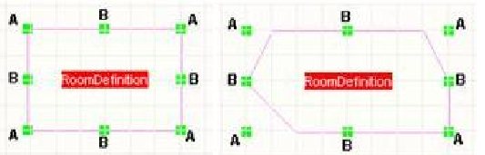
放置矩形ROOM:
1、单击菜单Design » Rooms » Place Rectangular Room 运行命令之后光标变成十字,进入 Room 放置模式:
2、定位并单击 (或按 ENTER 键) 确定 Room 的第一个边角。
3、移动光标调整 Room 的大小,然后单击 (或按 ENTER 键)放置 Room 的斜对角,从而完成一个 Room 的放置。
4、继续放置其它的 room,或右键单击或按 ESC 键退出放置 Room 模式
放置多边形 Room:单击菜单 Design » Rooms » Place Polygonal Room 运行命令之后光标会变成十字形,进入 Room 放置模 式:
- 定位并单击 (或按ENTER键) 确定Room的第一个边角。
- 定位光标,单击 (或按 ENTER 键)定义多边形的一系列的端点。
- 一旦结束放置最后一个端点,右键单击 (或按 ESC) 退出放置 Room 模式。没有必要手动闭合多边形,软件会自动连接起始点和终止点闭合多边形。
- 继续放置多边形 room,或右键单击 (或按 ESC) 退出放置 Room 模式。
定义 Room 外形时,可以使用以下的快捷键:SHIFT+ Spacebar 在多种转角模式之间切换,包括:任意角度,45°,45°圆弧,90°和 90°圆弧。圆弧半径可以通过 SHIFT+. (句号) 或 SHIFT+, (逗号) 变大或变小。 使用 Spacebar 在转角方向之间切换。在放置时使用 BACKSPACE 键,可以删除刚刚放置的上一个端点,重复该操作可以删除多边形,返回起始点。
使用菜单或工具栏命令创建 Room 非直角的、直角的和矩形 Room :可以通过在设计空间选择元器件来自动创建。它们由 Design » Rooms 的子菜单执行,相关命令包括:
从选择的零件创建非直角ROOM-------Create Non-Orthogonal Room from select components
从选择的零件创建直角ROOM------- Create Orthogonal Room from selected components
从选择的零件创建矩形ROOM--------Create Rectangle Room from selected components
上述三种情况下的创建方法都是一样的:
- 保证所有期望包含在 Room 中的的元件被选中。
- 执行相关的命令 Design » Rooms » Create … Room from selected components。 一个新的 Room 和 Component Class 会自动创建,Room 尺寸会按照元件边界裁剪到适合所有选 中的元件,并且关联到 Component Class。
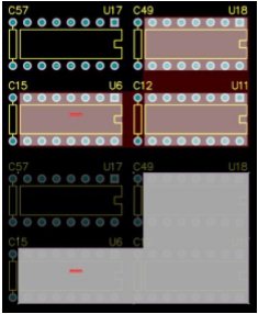
上图:选择3个芯片,创建直角的ROOM
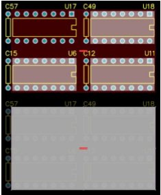
上图:选择3个芯片,创建矩形ROOM。注意 U17 不包含在 Rectangular Room 中,即使它被 Room 包围。这是因为 U17 在运 行命令之前并未选中。
在PCB主工作区每创建或放置一个 Room图形 时,会在design-----rools----placement-------room definition自动产生与这个 Room关联的设计规则。反之,当用户在上述位置添加一个 Room 新规则,在PCB主工作区也会相应的创建一个 Room空间。查看ROOM空间的设计规则单击菜单design------rools------placement-------room definition:见下图左侧。
怎样通过添加一个ROOM规则------实现在PCB主工作区添加一个ROOM:
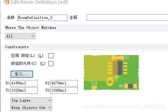
在下图 PCB Rules and Constraints Editor对话框的Placement列表的Room Definition入口右键单击, 在右键菜单中选择 New Rule 命令来添加一个新的 Room 定义。新的 Room 会被添加到左侧的文件树中,并显示在下图右侧对话框主编辑窗口的规则类型列表中。
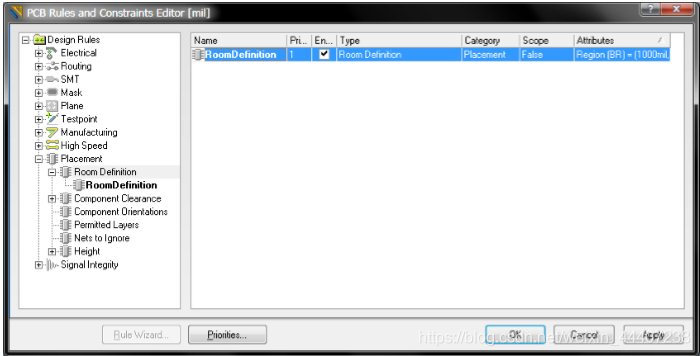
要编辑/定义新添加的 Room 的范围大小和在PCB板中的位置,点击它在文件树中的入口 (或双击汇总列表的设计规则入口) 打开 Room 定义的细节:见下图------点击 Define 按钮会跳转到PCB设计空间,用户在PCB编辑器设置 Room 的位置、外形和尺寸 - 无论是多边形 或矩形 Room 都一样。定义完 Room 的边界后会返回 PCB Rules and Constraints Editor 对 话框,点击 OK 退出对话框,满足设计规则的一个 Room 就会出现在设计空间。

在PCB编辑器中手工放置的ROOM,怎样与PCB编辑器中的元器件联系起来:
围绕一个或多个元器件放置矩形或多边形 Room,使这些元器件完全落入 Room 之中,这些元器件会自动与 Room 关联。
SCH原理图更新成PCB文件时,ROOM与零件的自动关联:
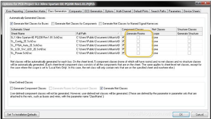
单击菜单project------project options------class generaiong-------生成room:打钩。在画完SCH原理图后------Design » UpdatePCB document-------执行完毕后,会为每个原理图页创建一个 Room,并 且关联到原理图页上所有的元件。
对ROOM属性的修改和编辑:
在PCB编辑器上绘制ROOM时,按下 TAB 键修改。
双击已经放置的ROOM。
右键点击 Room,在右键菜单中选择 Properties。
选择 Edit » Change 命令,然后点击需要编辑的 Room。 Room 定义的约束规则可以直接在 PCB Rules and Constraints Editor 对话框(Design » Rules) 中编辑
在PCB编辑器中选中一个 Room,无论该 Room 是何种类型,它周围会出现一些可编辑的端点句柄。见下图
拖动边角的端点 (A) 可以在水平和垂直方向同时缩放 Room 尺寸,拖动边线 (B) 可以在水平或垂 直方向改变 Room 尺寸。在拖动 Room 时可以将其旋转或翻转:按 SPACEBAR 逆时针旋转,按 SHIFT+SPACEBAR 顺时针旋转。旋转角度与 Rotation Step 值相 关,它在 Preferences 对话框(Tools » Preferences)的 PCB Editor » General 页面中定义。按 X 或 Y 键沿 X 轴或 Y 轴翻转对象。按 L 键翻转对象到电路板的另一面。如果 Room 有相关联的元器件,那些元器件会随着 Room 一起翻转。Room 对象也可以通过菜单命令 Design » Rooms » Move Room 来移动。
分配到一个 Room内的元件,在 Room 移动时元件也随之移动。如果希望移动一个 Room 而不移动元器件,设置方法:design-----rules------placement-------room definition-------勾选下图:锁定的元件。
勾选上图中:空间的锁定,启用 Room 的 Locked 选项可以锁定一个 Room,从而避免偶然移动它。如果 Room 初始使用 Create … Room from selected components 命令创建,任何 Wrap-based 命令将无效,因为 Room 的形状已经最优。
当使用 PCB Inspector 或 PCB List 面板编辑 Room 关联的 Room Definition 设计规则时, 选中的 Room 会显示为 Object Kind: Confinement Constraint Rule。
除了本身作为一个设计规则,Room 也可以在定义其它规则时作为一个对象。如果 Room 仅仅 作为其它规则的对象,它的 Room Definition 可以禁用。
下面两个查询语句用来定义 Room 的范围:
a) TouchesRoom(RoomName) -用于查找完全或部分位于 Room 中的对象。
b) WithinRoom(RoomName) -用于查找完全位于 Room 中的对象。
Room 可以用来定义电路板上自动走线或不走线的区域。相关命令可以从 Room 相关的右键菜单访问,或通过 Auto Route » Room and Tools » Unroute » Room 访问。
2.PCB添加图片或logo
3.四层高速dsp开发板制作
4.飞线的显示和隐藏
5.如何标注PCB板子的尺寸
五、经验与感悟
1.PCB大神总结5大设计经验! 真得很受用!
原文出处
PCB就好比电子电路的骨架和神经脉络,在电子工程项目中起着举足轻重的作用,但很多人对PCB设计并不了解或了解不够。
我在大学那时候,就对电路板设计、硬件电路设计特别感兴趣,也学得比较认真。当时觉得毕业后能找到一份坐在办公室进行计算机绘图的工作是多么好。毕业后,也如愿进入了东莞一家汽车电子公司,从事电子研发的工作,包括制作BOM表、样机调试和PCB绘图工作。当时2002年毕业时,还没有PCB工程师这个工种,基本上就是什么事情都要会一点,包括原理图绘制、器件选型、PCB绘图、样板焊接、调试、BOM制作、作业指导书等,也从此走上了电子研发这条路。
①.原理图
尽管优良的原理图不能保证好的布线,但是好的布线开始于优良的原理图。在绘制原理图时要深思熟虑,并且必须考虑整个电路的信号流向。如果在原理图中从左到右具有正常稳定的信号流,那么在PCB上也应具有同样好的信号流。在原理图上尽可能多给出有用的信息。因为有时候电路设计工程师不在,客户会要求我们帮助解决电路的问题,从事此工作的设计师、技术员和工程师都会非常感激,也包括我们。除了普通的参考标识符、功耗和误差容限外,原理图中还应该给出哪些信息呢?下面给出一些建议,可以将普通的原理图变成一流的原理图。加入波形、有关外壳的机械信息、印制线长度、空白区;标明哪些元件需要置于PCB上面;给出调整信息、元件取值范围、散热信息、控制阻抗印制线、注释、扼要的电路动作描述……(以及其它)。
②.都别信
如果不是你自己设计布线,一定要留出充裕的时间仔细检查布线人的设计。在这点上很小的预防抵得上一百倍的补救。不要指望布线的人能理解你的想法。在布线设计过程的初期你的意见和指导是最重要的。你能提供的信息越多,并且整个布线过程中你介入的越多,结果得到的PCB就会越好。给布线设计工程师设置一个暂定的完成点——按照你想要的布线进展报告快速检查。这种“闭合环路”方法可以防止布线误入歧途,从而将返工的可能性降至最低。需要给布线工程师的指示包括:电路功能的简短描述,标明输入和输出位置的PCB略图,PCB层叠信息(例如,板子有多厚,有多少层,各信号层和接地平面的详细信息——功耗、地线、模拟信号、数字信号和RF信号);各层需要那些信号;要求重要元件的放置位置;旁路元件的确切位置;哪些印制线很重要;哪些线路需要控制阻抗印制线;哪些线路需要匹配长度;元件的尺寸;哪些印制线需要彼此远离(或靠近);哪些线路需要彼此远离(或靠近);哪些元器件需要彼此远离(或靠近);哪些元器件要放在PCB的上面,哪些放在下面。永远不要抱怨需要给别人的信息太多——太少吗?是;太多吗?不。
分享一条学习经验:大约10年前,我设计一块多层的表面贴电路板——板子的两面都有元件。用很多螺钉将板子固定在一个镀金的铝制外壳中(因为有很严格的防震指标)。提供偏置馈通的引脚穿过板子。该引脚是通过焊接线连接到PCB上的。这是一个很复杂的装置。板子上的一些元件是用于测试设定(SAT)的。但是我已经明确规定了这些元件的位置。你能猜出这些元件都安装在什么地方吗?对了,在板子的下面。当产品工程师和技术员不得不将整个装置拆开,完成设定后再将它们重新组装的时候,显得很不高兴。从那以后我再也没有犯过这种错误了。
③.位置
正像在PCB中,位置决定一切。将一个电路放在PCB上的什么位置,将其具体的电路元件安装在什么位置,以及其相邻的其它电路是什么,这一切都非常重要。
通常,输入、输出和电源的位置是预先确定好的,但是它们之间的电路就需要“发挥各自的创造性”了。这就是为什么注意布线细节将产生巨大回报的原因。从关键元件的位置入手,根据具体电路和整个PCB来考虑。从一开始就规定关键元件的位置以及信号的路径有助于确保设计达到预期的工作目标。一次就得到正确的设计可以降低成本和压力——也就缩短了开发周期。
另外,说点有意思的,PCB板上那些“特殊焊盘“
第一个,泪滴焊盘

泪滴是焊盘与导线或者是导线与导孔之间的滴装连接过度,设置泪滴的目的是在电路板受到巨大外力的冲撞时,避免导线与焊盘或者导线与导孔的接触点断开,另外,设置泪滴也可使PCB电路板显得更加美观。
teardrop的作用是避免信号线宽突然变小而造成反射,可使走线与元件焊盘之间的连接趋于平稳过渡化,解决了焊盘与走线之间的连接容易断裂的问题。
1、焊接上,可以保护焊盘,避免多次焊接是焊盘的脱落
2、加强连接的可靠性(生产是可以避免蚀刻不均,过孔偏位出现的裂缝等)
3、平滑阻抗,减少阻抗的急剧跳变在电路板设计中,为了让焊盘更坚固,防止机械制板时焊盘与导线之间断开,常在焊盘和导线之间用铜膜布置一个过渡区,形状像泪滴,故常称做补泪滴( Teardrops )
第二个,放电齿

This is called a discharge tooth, discharge gap or spark gap. The spark gap is a pair of triangles with sharp angles pointing to each other. The fingertips are separated by a maximum of 10 mils and a minimum of 6 mils. One delta is grounded, and the other is connected to the signal line. This triangle is not a component, but is made by using a copper foil layer in the PCB routing process. These triangles need to be set on the top layer of the PCB (componentside) and cannot be covered by the solder mask.
1. In the switching power supply surge test or ESD test, high voltage will be generated at both ends of the common mode inductor and arcing will occur. If it is close to the surrounding devices, the surrounding devices may be damaged. Therefore, a discharge tube or varistor can be connected in parallel to limit its voltage, thereby playing the role of arc extinguishing. The effect of placing lightning protection devices is very good but the cost is relatively high.
2. Another method is to add discharge teeth at both ends of the common-mode inductor during PCB design, so that the inductor discharges through the two discharge tips, avoiding discharge through other paths, so as to minimize the impact on surrounding and subsequent devices.
The discharge gap does not require additional cost. It can be drawn when drawing the pcb board, but it is important to note that this type of discharge gap is an air-type discharge gap, which can only be used in an environment where ESD is occasionally generated. If used in occasions where ESD occurs frequently, carbon deposits will occur between the two triangular points due to frequent discharges between the discharge gaps, which will eventually cause a short circuit in the discharge gap, and cause permanent short-circuit of the signal line to the ground. Resulting in system failure.
In fact, PCB design has a lot of fun, and only when you practice it will you have a deep understanding. Seeing this article, if friends have any feelings about PCB design, you can leave a message below the comments to communicate.