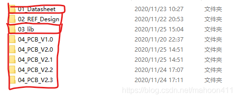
1. File structure of the project
When designing a PCB project, the file structure is mainly divided into four modules
- The first folder is used to store the data sheet of the chip used when designing the PCB.
- The second folder is used to store the reference design used when designing the PCB, including the minimum system circuit diagram of the chip used, various specification manuals, and PCBs designed by others.
- The third folder is used to store the schematic library and package library.
- The fourth folder is used to store AD project files. It is best to save as a version every time you make some changes.
2. Schematic design
First, design the schematic diagram.
Before that, I mentioned that the principle library of the chip can be downloaded from the Litron Mall, and the principle library can be downloaded by using the export function of Litron EDA.
2.1 Minimal system
As shown in the figure below, the MCU of this module uses STM32F103RCT6, which is a 64-pin MCU. It’s not that you have to use 64-pin to achieve, 48-pin is also possible, and the utilization rate is higher, just because you have STM32F103RCT6 on hand, and this module is only used for practice, so I use this chip As the master chip.
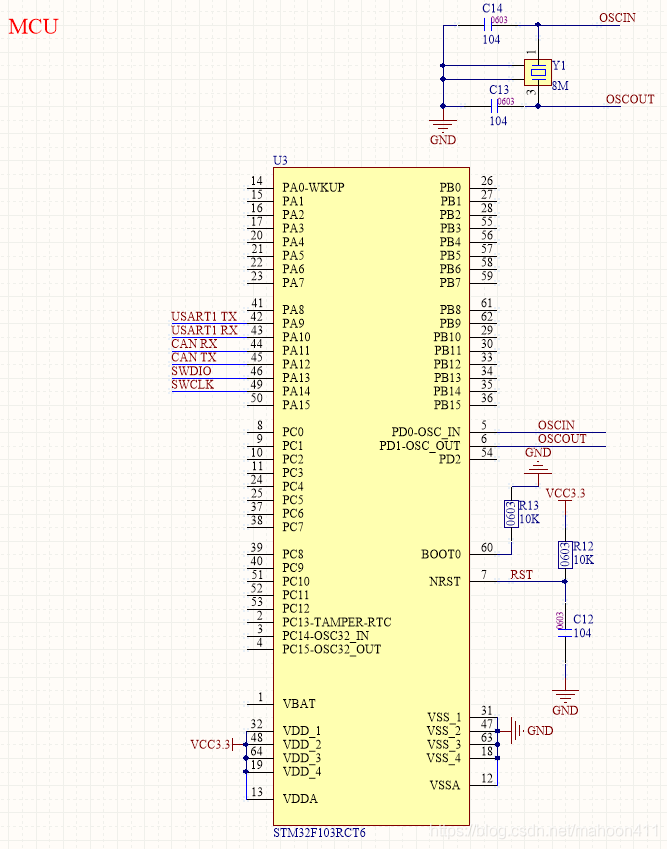
In the smallest system, use 3.3V power supply, 8M external crystal oscillator circuit, and use pull-down resistors for BOOT0 and pull-up resistors for NRST.
In order to reduce the size of the module and take into account the power consumption, 0603 is used for the packaging of resistors and capacitors.
2.2 USB to serial port
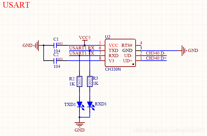
Generally see USB to serial port circuit, the chip used is CH340G, but because this module is only an experimental module, it does not need to use many functions, so after consulting the data, I chose a smaller size but can just meet the needs The CH330N module.
An external LED is connected to the TXD and RXD pins of CH330N, so that when the module starts communication, the indicator light will light up: when the host computer sends data, the TXD1 indicator light is on; when the host computer receives data, RXD1 The indicator light is on.
When designing the driving circuit of the LED lamp at the beginning, it was considered that if the resistance is connected directly and then the LED lamp is driven, a lot of current will be consumed, which may affect the transmission and reception of data. Therefore, another idea is to use MOS tubes to drive LED lights. This solution consumes very little current and will not affect data transmission and reception. However, the disadvantage is that it occupies a larger area and the circuit is more complicated. Finally, after consulting various reference circuits on the Internet, it was found that there is a circuit that directly drives the LED lamp, so the solution of directly driving the LED lamp was finally adopted.
2.3 CAN communication

CAN transceiver uses TJA1050.
The external interface of CAN uses a 5-pin connector, which is designed to match the housing of the CAN to USB module.
Generally speaking, an isolation circuit should be added to the CAN communication part, such as optocoupler isolation or resistance isolation or magnetic coupling isolation. But because this module is only an experimental module, no isolation circuit is designed.
The SW1 switch is to allow one end of the CAN bus to choose to mount or not mount a 120Ω resistor according to the situation.
2.4 JLINK emulator
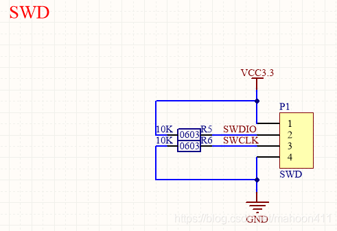
In order to further reduce the size, the SWD mode of the J-Link emulator is selected. This circuit can be designed according to the difference between using J-Link emulator to select JTAG mode and SWD mode in the blog STM32 .
2.5 Power
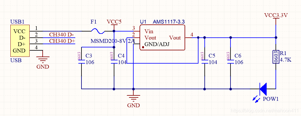
This module uses external USB power supply. Since the USB power supply voltage is 5V, it is necessary to use AMS1117-3.3 to convert 5V to 3.3V.
An external fuse F1 is connected to ensure the safety of the circuit.
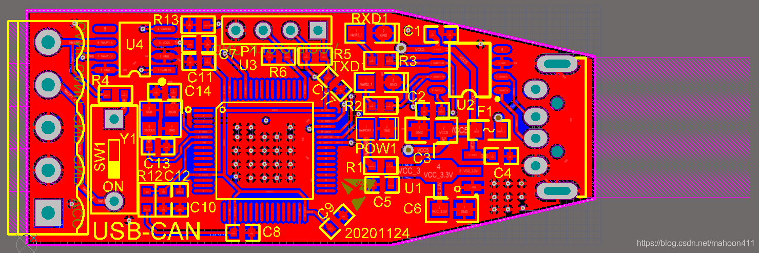
3. PCB design
Note that the package library of the chip can also be downloaded from the Litron Mall, and the package library can be downloaded using the export function of Litron EDA.
3.1 Layout
After the schematic is designed, compile it, and after the compiling is passed, it can be imported into the pcb file. But before importing the components, we'd better perform the size design of the pcb board.
The PCB size diagram designed according to the shell of the CAN to USB module is shown in the figure below.

Draw the outer border of the PCB in the keepout layer according to the size drawing.

Then select all the borders and click define from selected objects.

Complete the shape and size design of the pcb board. Next, layout.

After the design is completed, the components can be imported into the pcb.
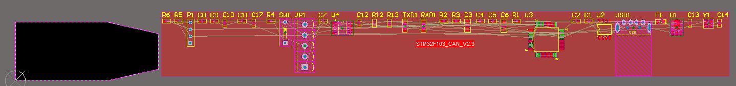
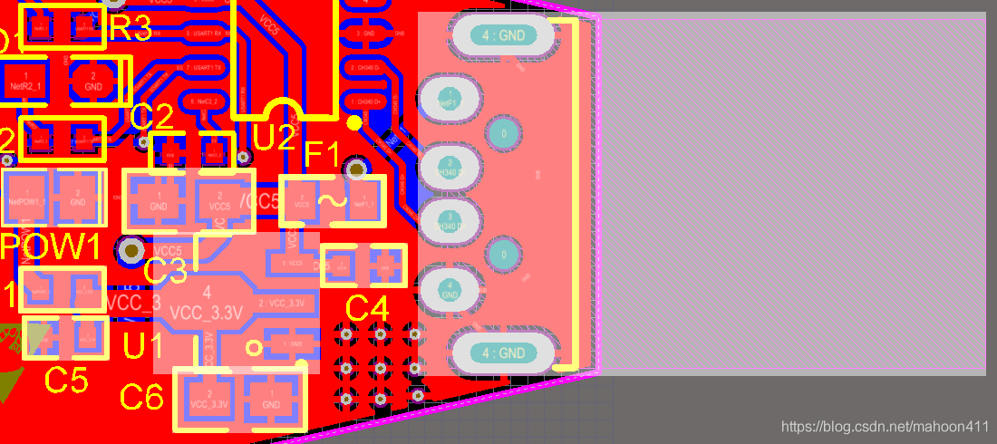
Pay attention to the layout, all components in each small module, it is best to put together in the layout. Take the power supply part in the PCB diagram that has been designed as an example. The layout of the power supply part is shown in the figure below.
3.2 Wiring
This module adopts double-layer board design.
When punching holes, pay attention: the signal wire uses a via with an inner diameter of 0.2mm and an outer diameter of 0.45mm; the power wire uses a via with an inner diameter of 0.5mm and an outer diameter of 1mm. And the via hole should be farther away from the pad.
When wiring, pay attention: the signal wire uses 0.2mm wire; the power wire is selected according to the situation, at least 0.5mm wire.
CANL and CANH should use 0.5mm wire.
3.3 Copper coating
The front and back of this module are coated with copper.
Pay attention to the connection with the GND network when applying copper. For example, the settings for copper-clad top layer are shown in the figure below.

The pcb board with copper on the front and back is shown in the figure below.