Problem background
When learning FSMC to control external NOR memory, we saw that in NOR multiplexing interface mode, AD signal [15:0] is multiplexed. That is to say, if the latch is not used: when NADV is low, the address signal Ax appears on ADx (x=0...15), and when NADV becomes high, the data signal Dx appears on ADx. If a latch is used: Ax and Dx can be obtained on ADx at the same time.
Multiplexing mode: The lower 16-bit data/address lines are multiplexed. In this mode, it is recommended to use an address latch to distinguish data from address.
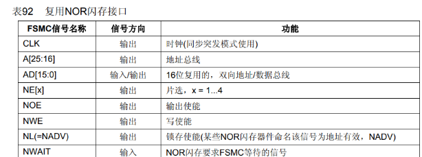
The level of the NADV signal determines whether the data is data or address. This is easy to understand.
So what is a latch, and why can we get Ax. at the same time by using a latch?
Introduction
Take the latch-74HC573D as an example

The truth table

74HC573 chip is a latch. Simply put, the input pins D1~D8 control the output pins Q1~Q8. The values of OE and LE will affect the input data and control the output data.
OE: output enable output enable (low level active)
LE: latch enable latch enable
When OE is L and LE is H, it is following mode, and output data = input data.
When OE is L and LE is L, it is latch mode, and the output data = the input data at the previous moment.