If the name written in the article, "a senior verification engineer to tell you how to design an article by register", then this article is likely to be passed to the major BBS, get good traffic. But when I think of me I had a lot better than my verification engineer, claiming they were not so, I think this title I really can not afford, ha ha!
Concept Register (segment domains) access attribute
A typical register are defined as follows.
Storage Name: System Configuration Register [0xC800_0000]
| Domain name segments |
Domain section range |
Access Properties |
Defaults |
description |
| rsv |
31-7 |
RO |
0 |
Retention |
| 6-4 |
RW |
0 |
Start cores 0: rar 1:mpeg4 2:avi 3:3gp 4:flv 5: the others:rsv |
|
| rsv |
3-1 |
RO |
0 |
Retention |
| mode_type |
0 |
RW |
0 |
0: Normal mode 1: Test mode |
Access Domain section, from the processor (e.g., CPU) of the end look. In mode_type an example, the access attribute field section is RW (read-write), indicating that the value field segment may be written either the processor, the processor may be read out. In general, access to the register access attribute register fields coincide segment attributes. For register reserved field, a general processor operation information is not reserved field segments, reserved fields that can only be read default value of "0" may be reserved field access attribute labeled "the RO (Read Only) . "
Due to the presence of the reserved field in the above examples, the "System Configuration Register" of the access attribute RW, wherein the domain segment mode_type and video_format access attributes are RW, but the access attribute of the reserved field is the RO, i.e., the register access attribute and domain segments exist access inconsistent property cases.
For convenience of description, all "attribute register access" will hereinafter be especially effective as an "access attribute domain segment."
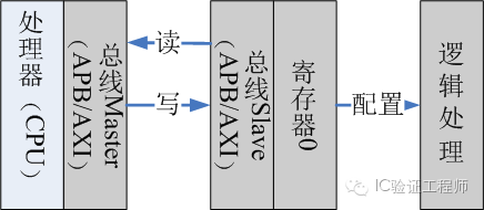
Register access structure

As shown, the bus Slave processor (CPU) accessible through its bus Master logic design. Bus Slave register bus access analytical, if it is a write operation, is generally configured to convert logical processing, if it is a read operation, the read result is reported general conversion logic processing.
For convenience of description hereinafter, the processor will write the information called "data", and the existing information stored in an internal logic design, referred to as "segment value field."
UVM -defined access attribute register
UVM定义的寄存器访问属性共有25个。如果想一下记住25个访问属性,还是比较难的。因此,我们需要对访问属性先做一个归纳总结:
1、 所有包括R的访问属性,会将寄存器的“域段值”读出给处理器;
2、 所有包括W的访问属性,会将处理器的“数据”,传递给寄存器域段处理,但不一定是简单的赋值操作;
3、 读操作的处理范围是整个寄存器(因为读操作无法区分读哪个域段,不读哪个域段);
4、 写操作的处理范围可以是整个寄存器,也可以是某个域段,当需要区分域段时,需要通过1(或0)标记哪个域段信息被操作;
5、 所有包括“C”的访问,将清除(清0)对应处理范围的信息,处理范围可能是整个寄存器,也可能是整个域段;
6、 所有包括“S”的访问,将置位(置1)对应处理范围的信息,处理范围可能是整个寄存器,也可能是整个域段;
7、 所有包括“T”的访问,将翻转(0->1,1->0)对应处理范围的信息,处理范围可能是整个寄存器,也可能是整个域段;
如果您已经理解以上7点,那么我们可以继续学习UVM的寄存器属性了。
UVM定义的寄存器访问属性如下所示。
| ”RO” | W: no effect, R: no effect |
| ”RW” | W: as-is, R: no effect |
| ”RC” | W: no effect, R: clears all bits |
| ”RS” | W: no effect, R: sets all bits |
| ”WRC” | W: as-is, R: clears all bits |
| ”WRS” | W: as-is, R: sets all bits |
| ”WC” | W: clears all bits, R: no effect |
| ”WS” | W: sets all bits, R: no effect |
| ”WSRC” | W: sets all bits, R: clears all bits |
| ”WCRS” | W: clears all bits, R: sets all bits |
| ”W1C” | W: 1/0 clears/no effect on matching bit, R: no effect |
| ”W1S” | W: 1/0 sets/no effect on matching bit, R: no effect |
| ”W1T” | W: 1/0 toggles/no effect on matching bit, R: no effect |
| ”W0C” | W: 1/0 no effect on/clears matching bit, R: no effect |
| ”W0S” | W: 1/0 no effect on/sets matching bit, R: no effect |
| ”W0T” | W: 1/0 no effect on/toggles matching bit, R: no effect |
| ”W1SRC” | W: 1/0 sets/no effect on matching bit, R: clears all bits |
| ”W1CRS” | W: 1/0 clears/no effect on matching bit, R: sets all bits |
| ”W0SRC” | W: 1/0 no effect on/sets matching bit, R: clears all bits |
| ”W0CRS” | W: 1/0 no effect on/clears matching bit, R: sets all bits |
| ”WO” | W: as-is, R: error |
| ”WOC” | W: clears all bits, R: error |
| ”WOS” | W: sets all bits, R: error |
| ”W1” | W: first one after HARD reset is as-is, other W have no effects, R: no effect |
| ”WO1” | W: first one after HARD reset is as-is, other W have no effects, R: error |
| ”NOACCESS” | W: no effect, R: no effect |
寄存器访问属性的应用
RW(读写)
RW寄存器是逻辑设计中数量最多的寄存器,一般用于配置操作。其中的读操作是可测试性设计,写入的寄存器,处理器可以通过读取操作,判断写入信息是否正确。
有“高人”曾建议,配置寄存器就应该采用“WO只写”方式,这样可以节省寄存器资源。我当时真的感到“天雷滚滚”!不怕被测试、软件,以及项目经理骂死,就这么设计好了。省的那点资源,不够费的功夫。
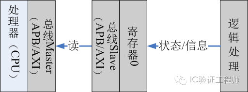
RO(只读)
RO寄存器是逻辑设计中数量第二多的寄存器,一般用于状态指示,或者信息采样。
状态指示举例:当前的时钟是否锁定(PLL_LOCK);当前的状态机状态(FSM_State);
信息采样举例:当前处理数据的平均功率统计(averagepower)。
RC(读清)
RC寄存器,读操作后,域段信息就被清除。应用RC寄存器的考虑因素包括:
从设计便利性考虑:一段时间的统计信息,如计数值,或者平均功率,读操作完成后,数据清零,重新统计;
从信息的重要性考虑:相对不是特别重要的信息,一般可以采用读清操作。
RC寄存器与RO寄存器的结构基本一致,仅多了一步清除操作。
RS(读置位)
与RC的应用场景类似,有时候计数器置位后,下一次计数则从0xffff直接跳到0,比较方便。但是,本能上不喜好这样的设计,没有任何特殊理由。
WC(写清)
主要与RC(读清)寄存器对比,相比较读清,写清可以在软件确信获取到信息后,再清除信息。需要注意的是,WC(写清)是与RC(读清)做选择,而不是和W1C(写1清)做选择。因为WC和RC都是对整个寄存器的操作,而W1C是对域段的操作,应用场景完全不同。

W1C(写1清)
最常用于“中断状态指示寄存器”。
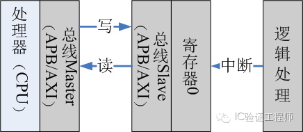
当中断发生时,逻辑发送中断“脉冲”给寄存器域段缓存。处理器收到中断线指示(中断使能场景)后,读取相应的“中断状态指示寄存器”,获取是哪个信息导致的中断。处理器依次处理中断对应信息,完成中断处理程序后,向对应域段的写1,清除对应域段。

一般W1C寄存器,与某个RW寄存器的域段一一对应,该RW寄存器为“中断状态指示使能寄存器”,一个bit的使能,对应一个bit的中断状态指示。
写1清的好处是,仅操作对应域段,而不影响其他域段的中断信息。

W1C(写1清)要小心“电平指示”中断。
对于“脉冲”指示的中断,中断信息缓存在寄存器域段里,如果清中断,系统中就不再有中断指示。但是,对于“电平指示”的中断,仅仅清除寄存器域段中的指示是不够的,还需要清除逻辑处理发出的持续电平信号。否则,即使清除了寄存器域段中的中断指示,逻辑处理的中断电平又会立刻将寄存器中的中断指示拉起。导致最终陷入“清中断->重新拉起中断”的死循环。

W1T(写1翻转)
一个非常有意思的寄存器访问属性,最常用于“总线测试寄存器”。举例如下:

当“域段值”为8’hFF时,写入8’h55,读出8’hAA,证明总线(APB/AXI)读写正常。
W1(只写1次)
一般这样的寄存器应用于做“一次”操作的判断(flag)。应用该寄存器的需求分析:
1、 从便利性的角度分析:可以多个软件进程调用写,只要有一个写操作,写操作就记录,且屏蔽后续的写操作。在某些场景下,这样的设计会比较方便;
2、 从“安全性”的角度分析:某些特殊信息,如DDR初始化启动指示等,上电后,仅操作一次。
但是,从设计角度讲,这样的设计有些过于严格要求硬件,而放松软件。但是,硬件如何设计不合理,软件是没有办法挽回的。例如DDR初始化,可能在某些场景,需要执行两次,如果软复位操作不到对应寄存器,系统就可能挂死。因此,要慎用W1(只写1次)访问属性的寄存器。
其余寄存器访问属性
其余寄存器访问属性,不是特别常见,本文就不再赘述。虽然更多的寄存器属性,可以带来应用上的方便,但是也会带来理解上的障碍。从沟通的角度来看,我建议尽量少用不常见的寄存器属性。当然,哪些寄存器访问属性是常用的,哪些是不常用的,这个问题可以好好探讨。
