A rectifying circuit (rectifier circuit) is an important application of the diode, which is a function of the alternating current into direct current, the structure below shows the basic block diagram of a conventional DC power supply:
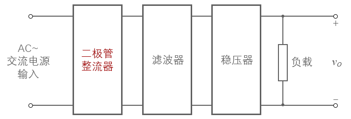
Figure 2-3.01
This section we want to analyze in detail, is the figure of a diode rectifier (diode rectifier) section. As power diode rectifier diode is usually used, its power and the maximum positive value of the bias current is much greater than the fast diode typically used as switches, power diodes have commonly used: 1N4001 ~ 1N4007 series. Rectifier circuit commonly used half-wave rectification and full-wave rectified two kinds following description separately.
1. half-wave rectifier
Half-wave rectifier (half-wave rectification) of the circuit is very simple, as shown below:
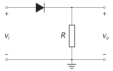
Figure 2-3.02
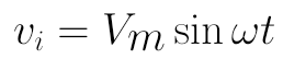
Provided the input voltage is sinusoidal voltage transformer through the transformer, the expression is:
When the input voltage V I when the positive half cycle and is larger than 0.7V, the diode is turned on, then the output voltage V O is only than V I small 0.7V; when the input voltage is less than 0.7V (the negative half cycle and throughout the positive half portion is less than 0.7V, ), the diode is turned off, the output voltage V O is 0, comparison input and output waveform diagram as shown below:
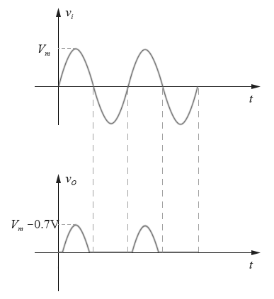
Figure 2-3.03
Of course, only the waveform of FIG. Our hypothetical ideal diode, in fact, due to the nonlinear volt-ampere characteristic of the diode, the difference between the input voltage and the output voltage at the peak to be larger, the true input voltage and the output voltage after the comparison is an enlarged waveform such as shown below, the following input V m of 5V oscilloscope waveform observed:

Figure 2-3.04
When the input voltage V m much greater than 0.7V, in fact, this slight deviation is negligible.
Further, think again at half-wave rectifier, the diode reverse bias peak voltage (PIV), when the input voltage is in a negative half cycle, almost all of the reverse bias voltage is applied to the diode, the diode reverse bias voltage parameters requirements are:
PIV rating ≥ V m (half-wave rectification)
General half-wave rectifier and is not used in practice, because efficiency is too low, the entire negative half cycle are wasted. So the half-wave rectification described above, is only used to help understand the concept of preliminary rectified, the real and practical full-wave rectification is to introduce the following.
2. full-wave rectification
(1) full-wave bridge rectifier
The most common bridge (bridge network) full-wave rectification (full-wave rectification) circuit diagram as shown below:

Figure 2-3.05
When the input voltage is in the positive half cycle, the diode D 2 and D . 3 is turned on, the diode D . 1 and D . 4 OFF. When the input voltage is in a negative half cycle, diodes D . 4 and D . 1 is turned on, the diode D 2 and D . 3 off. Current flow are shown below:
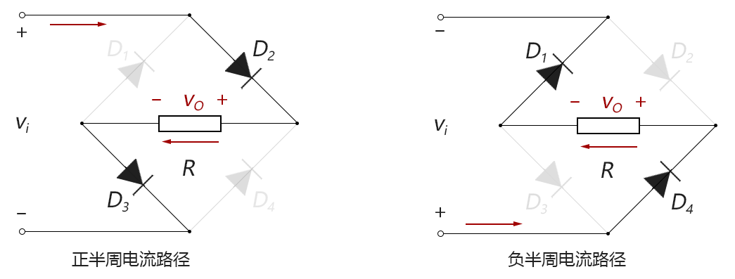
Figure 2-3.06
Note that in the figure above, the direction of current flowing through the load resistance R is always right to left, the voltage polarity on R is always in one direction. Further, the current path to go through the two diodes, the output voltage will drop 2 0.7V (i.e., 1.4V) than the input voltage, input and output waveforms of the final full-wave rectified looks like this:
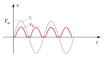
Figure 2-3.07
When the input voltage V m much greater than 1.4V, this can be ignored 1.4V, the output voltage waveform approximated that is this:

Figure 2-3.08
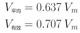
The theoretical formula for the AC circuit, "average" and "valid value" can be obtained the following results:
Finally, look for full-wave rectifying diode parameters required PIV to an example positive half cycle (where D 2 and D . 3 is turned on, a short circuit can be regarded as approximate), the following figure can be seen that both D . 1 or D 4 , are under almost all V I voltage
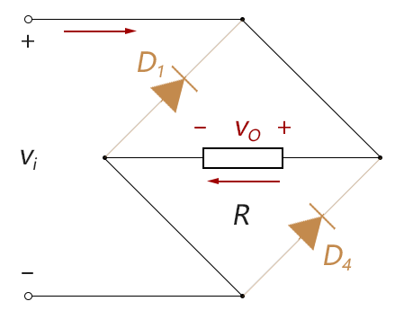
Figure 2-3.09
Therefore, the selection of the full-wave rectifier diode, PIV parameter requirements:
PIV rating ≥ V m (full-wave bridge rectifier)
(2) center-tapped transformer full-wave rectifier
Another common full-wave rectification circuit using a center-tapped transformer (center-tapped transformer) a rectifier circuit, also called CT full-wave rectified, as shown below:
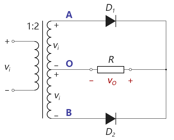
Figure 2-3.10
变压器的初级和次级线圈绕组的匝数为1:2,次级线圈上会产生2倍于vi的电压,但是对于中间的抽头O点引出后,无论是AO之间还是BO之间,都只有次级线圈的一半匝数,故它们的电压vAO和vBO都等于vi
当输入电压处于正半周时,二极管D1导通,D2截止,负载R上的电压为vo等于次级线圈的一半(即AO之间)的电压,此值大小等于vi,流过R的电流方向为从右至左;当输入电压处于负半周时,二极管D2导通,D1截止,负载R上的电压为vo等于次级线圈的另一半(即BO之间)的电压,此值大小也等于vi,流过R的电流方向同样为从右至左。 输出电压vo的波形如下图所示:
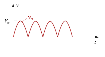
图 2-3.11
中心抽头变压器全波整流对于二极管PIV参数的要求与桥式整流不同,从前面图中可以看到,对于每个二极管,当其反偏时,要承受整个整个次级线圈的反偏电压,即2倍的vi,所以对于中心抽头变压器全波整流二极管的选型要求为:
PIV额定值 ≥ 2Vm (中心抽头变压器全波整流)
( end of 2-3 )